
User manual


Table Of Contents
- Zynq-7000 All Programmable SoC
- Table of Contents
- Ch. 1: Introduction
- Ch. 2: Signals, Interfaces, and Pins
- Ch. 3: Application Processing Unit
- Ch. 4: System Addresses
- Ch. 5: Interconnect
- Ch. 6: Boot and Configuration
- Ch. 7: Interrupts
- Ch. 8: Timers
- Ch. 9: DMA Controller
- Introduction
- Functional Description
- DMA Transfers on the AXI Interconnect
- AXI Transaction Considerations
- DMA Manager
- Multi-channel Data FIFO (MFIFO)
- Memory-to-Memory Transfers
- PL Peripheral AXI Transactions
- PL Peripheral Request Interface
- PL Peripheral - Length Managed by PL Peripheral
- PL Peripheral - Length Managed by DMAC
- Events and Interrupts
- Aborts
- Security
- IP Configuration Options
- Programming Guide for DMA Controller
- Programming Guide for DMA Engine
- Programming Restrictions
- System Functions
- I/O Interface
- Ch. 10: DDR Memory Controller
- Introduction
- AXI Memory Port Interface (DDRI)
- DDR Core and Transaction Scheduler (DDRC)
- DDRC Arbitration
- Controller PHY (DDRP)
- Initialization and Calibration
- DDR Clock Initialization
- DDR IOB Impedance Calibration
- DDR IOB Configuration
- DDR Controller Register Programming
- DRAM Reset and Initialization
- DRAM Input Impedance (ODT) Calibration
- DRAM Output Impedance (RON) Calibration
- DRAM Training
- Write Data Eye Adjustment
- Alternatives to Automatic DRAM Training
- DRAM Write Latency Restriction
- Register Overview
- Error Correction Code (ECC)
- Programming Model
- Ch. 11: Static Memory Controller
- Ch. 12: Quad-SPI Flash Controller
- Ch. 13: SD/SDIO Controller
- Ch. 14: General Purpose I/O (GPIO)
- Ch. 15: USB Host, Device, and OTG Controller
- Introduction
- Functional Description
- Programming Overview and Reference
- Device Mode Control
- Device Endpoint Data Structures
- Device Endpoint Packet Operational Model
- Device Endpoint Descriptor Reference
- Programming Guide for Device Controller
- Programming Guide for Device Endpoint Data Structures
- Host Mode Data Structures
- EHCI Implementation
- Host Data Structures Reference
- Programming Guide for Host Controller
- OTG Description and Reference
- System Functions
- I/O Interfaces
- Ch. 16: Gigabit Ethernet Controller
- Ch. 17: SPI Controller
- Ch. 18: CAN Controller
- Ch. 19: UART Controller
- Ch. 20: I2C Controller
- Ch. 21: Programmable Logic Description
- Ch. 22: Programmable Logic Design Guide
- Ch. 23: Programmable Logic Test and Debug
- Ch. 24: Power Management
- Ch. 25: Clocks
- Ch. 26: Reset System
- Ch. 27: JTAG and DAP Subsystem
- Ch. 28: System Test and Debug
- Ch. 29: On-Chip Memory (OCM)
- Ch. 30: XADC Interface
- Ch. 31: PCI Express
- Ch. 32: Device Secure Boot
- Appx. A: Additional Resources
- Appx. B: Register Details
- Overview
- Acronyms
- Module Summary
- AXI_HP Interface (AFI) (axi_hp)
- CAN Controller (can)
- DDR Memory Controller (ddrc)
- CoreSight Cross Trigger Interface (cti)
- Performance Monitor Unit (cortexa9_pmu)
- CoreSight Program Trace Macrocell (ptm)
- Debug Access Port (dap)
- CoreSight Embedded Trace Buffer (etb)
- PL Fabric Trace Monitor (ftm)
- CoreSight Trace Funnel (funnel)
- CoreSight Intstrumentation Trace Macrocell (itm)
- CoreSight Trace Packet Output (tpiu)
- Device Configuration Interface (devcfg)
- DMA Controller (dmac)
- Gigabit Ethernet Controller (GEM)
- General Purpose I/O (gpio)
- Interconnect QoS (qos301)
- NIC301 Address Region Control (nic301_addr_region_ctrl_registers)
- I2C Controller (IIC)
- L2 Cache (L2Cpl310)
- Application Processing Unit (mpcore)
- On-Chip Memory (ocm)
- Quad-SPI Flash Controller (qspi)
- SD Controller (sdio)
- System Level Control Registers (slcr)
- Static Memory Controller (pl353)
- SPI Controller (SPI)
- System Watchdog Timer (swdt)
- Triple Timer Counter (ttc)
- UART Controller (UART)
- USB Controller (usb)
Zynq-7000 AP SoC Technical Reference Manual www.xilinx.com 428
UG585 (v1.11) September 27, 2016
Chapter 15: USB Host, Device, and OTG Controller
15.7.2 Endpoint Transfer Descriptor (dTD)
The dTD describes to the device controller the location and quantity of data to be sent/received for
given transfer. The DCD should not attempt to modify any field in an active dTD except the Next dTD
Pointer.
The dTD descriptors are illustrated in Table 15-14. The fields are detailed in Table 15-8 and described
in section 15.7.3 Endpoint Transfer Overlay Area.
15 Interrupt On Setup, IOS. This bit is used on control type endpoints to indicate if USBINT is set in
response to a setup being received.
14:0 Reserved. Field reserved and should be set to 0.
DWord 1: Current dTD Pointer
31:5 Current dTD Pointer. Pointer to the dTD that is represented in the transfer overlay area. This field
will be modified by the Device Controller to next dTD pointer during endpoint priming or queue
advance.
The current dTD pointer is used by the device controller to locate the transfer in progress. This word
is for the Device Controller hardware’s use only and should not be modified by the DCD.
4:0 Reserved. Field reserved and should be set to 0.
DWords 2 to 8: Overlay Area, refer to Table 15-15 USB Device Transfer Overlay.
DWord 9: reserved.
DWord 10: Setup Buffer Bytes 3:0
31:24
24:16
15:8
7:0
Byte 3
Byte 2
Byte 1
Byte 0
Table 15-13: USB Device dQH DWords 0 to 11: Descriptor Bit Details (Cont’d)
Bits Description
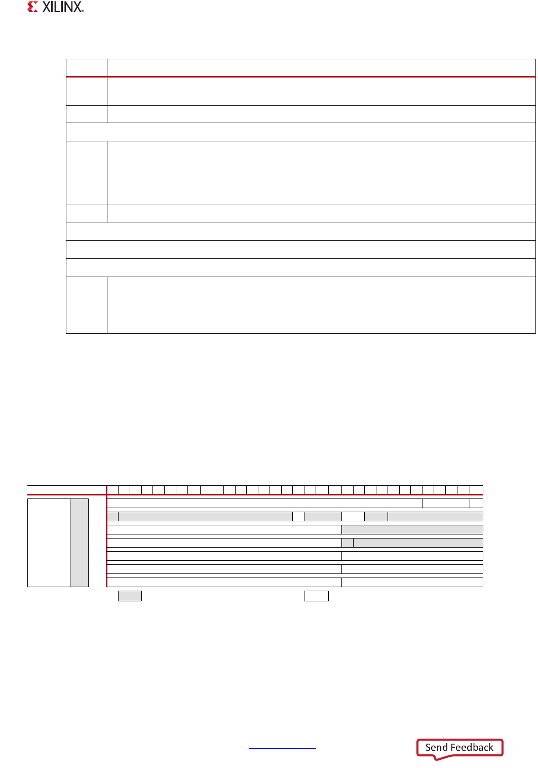
Table 15-14: USB Device Transfer Descriptor (dTD) Format
Reference Type 313029282726252423222120191817161514 13 121110 9 8 7 6 5 4 3 2 1 0 DWord
Table 15-15
Transfer Overlay Area
Next dTD Pointer 0000 T 0
0 Total Bytes
IOC
C_Page MultO 0 Status 1
Buffer Pointer (Page 0)
Current Offset 2
Buffer Pointer (Page 1)
R Frame Number 3
Buffer Pointer (Page 2) reserved 4
Buffer Pointer (Page 3) reserved 5
Buffer Pointer (Page 4) reserved 6
Device Controller Read/Write Device Controller Read-only