
User manual


Table Of Contents
- Zynq-7000 All Programmable SoC
- Table of Contents
- Ch. 1: Introduction
- Ch. 2: Signals, Interfaces, and Pins
- Ch. 3: Application Processing Unit
- Ch. 4: System Addresses
- Ch. 5: Interconnect
- Ch. 6: Boot and Configuration
- Ch. 7: Interrupts
- Ch. 8: Timers
- Ch. 9: DMA Controller
- Introduction
- Functional Description
- DMA Transfers on the AXI Interconnect
- AXI Transaction Considerations
- DMA Manager
- Multi-channel Data FIFO (MFIFO)
- Memory-to-Memory Transfers
- PL Peripheral AXI Transactions
- PL Peripheral Request Interface
- PL Peripheral - Length Managed by PL Peripheral
- PL Peripheral - Length Managed by DMAC
- Events and Interrupts
- Aborts
- Security
- IP Configuration Options
- Programming Guide for DMA Controller
- Programming Guide for DMA Engine
- Programming Restrictions
- System Functions
- I/O Interface
- Ch. 10: DDR Memory Controller
- Introduction
- AXI Memory Port Interface (DDRI)
- DDR Core and Transaction Scheduler (DDRC)
- DDRC Arbitration
- Controller PHY (DDRP)
- Initialization and Calibration
- DDR Clock Initialization
- DDR IOB Impedance Calibration
- DDR IOB Configuration
- DDR Controller Register Programming
- DRAM Reset and Initialization
- DRAM Input Impedance (ODT) Calibration
- DRAM Output Impedance (RON) Calibration
- DRAM Training
- Write Data Eye Adjustment
- Alternatives to Automatic DRAM Training
- DRAM Write Latency Restriction
- Register Overview
- Error Correction Code (ECC)
- Programming Model
- Ch. 11: Static Memory Controller
- Ch. 12: Quad-SPI Flash Controller
- Ch. 13: SD/SDIO Controller
- Ch. 14: General Purpose I/O (GPIO)
- Ch. 15: USB Host, Device, and OTG Controller
- Introduction
- Functional Description
- Programming Overview and Reference
- Device Mode Control
- Device Endpoint Data Structures
- Device Endpoint Packet Operational Model
- Device Endpoint Descriptor Reference
- Programming Guide for Device Controller
- Programming Guide for Device Endpoint Data Structures
- Host Mode Data Structures
- EHCI Implementation
- Host Data Structures Reference
- Programming Guide for Host Controller
- OTG Description and Reference
- System Functions
- I/O Interfaces
- Ch. 16: Gigabit Ethernet Controller
- Ch. 17: SPI Controller
- Ch. 18: CAN Controller
- Ch. 19: UART Controller
- Ch. 20: I2C Controller
- Ch. 21: Programmable Logic Description
- Ch. 22: Programmable Logic Design Guide
- Ch. 23: Programmable Logic Test and Debug
- Ch. 24: Power Management
- Ch. 25: Clocks
- Ch. 26: Reset System
- Ch. 27: JTAG and DAP Subsystem
- Ch. 28: System Test and Debug
- Ch. 29: On-Chip Memory (OCM)
- Ch. 30: XADC Interface
- Ch. 31: PCI Express
- Ch. 32: Device Secure Boot
- Appx. A: Additional Resources
- Appx. B: Register Details
- Overview
- Acronyms
- Module Summary
- AXI_HP Interface (AFI) (axi_hp)
- CAN Controller (can)
- DDR Memory Controller (ddrc)
- CoreSight Cross Trigger Interface (cti)
- Performance Monitor Unit (cortexa9_pmu)
- CoreSight Program Trace Macrocell (ptm)
- Debug Access Port (dap)
- CoreSight Embedded Trace Buffer (etb)
- PL Fabric Trace Monitor (ftm)
- CoreSight Trace Funnel (funnel)
- CoreSight Intstrumentation Trace Macrocell (itm)
- CoreSight Trace Packet Output (tpiu)
- Device Configuration Interface (devcfg)
- DMA Controller (dmac)
- Gigabit Ethernet Controller (GEM)
- General Purpose I/O (gpio)
- Interconnect QoS (qos301)
- NIC301 Address Region Control (nic301_addr_region_ctrl_registers)
- I2C Controller (IIC)
- L2 Cache (L2Cpl310)
- Application Processing Unit (mpcore)
- On-Chip Memory (ocm)
- Quad-SPI Flash Controller (qspi)
- SD Controller (sdio)
- System Level Control Registers (slcr)
- Static Memory Controller (pl353)
- SPI Controller (SPI)
- System Watchdog Timer (swdt)
- Triple Timer Counter (ttc)
- UART Controller (UART)
- USB Controller (usb)
Zynq-7000 AP SoC Technical Reference Manual www.xilinx.com 45
UG585 (v1.11) September 27, 2016
Chapter 2: Signals, Interfaces, and Pins
2.3 PS I/O Pins
A summary of the dedicated PS signal pins is shown in Table 2-2.
CAUTION! For MIO pins, the allowable Vin High level voltage depends on the settings of the
slcr.MIO_PIN_xx [IO_Type] and [DisableRcvr] bits. These restrictions and the restrictions for all I/O pins
are defined in the Zynq-7000 AP SoC data sheets. Damage to the input buffer can occur when the limits
are exceeded.
7z007s and 7z010 Devices
The 7z007s single core and 7z010 dual core CLG225 devices (225 pin packages) have fewer pins than
the other Zynq-7000 AP SoC devices (see Table 2-2). Details for DDR and MIO pins can be found in
Chapter 10, DDR Memory Controller and section 2.5.3 MIO Pin Assignment Considerations,
respectively. There is more information about the CLG225 devices in section 1.1.3 Notices.
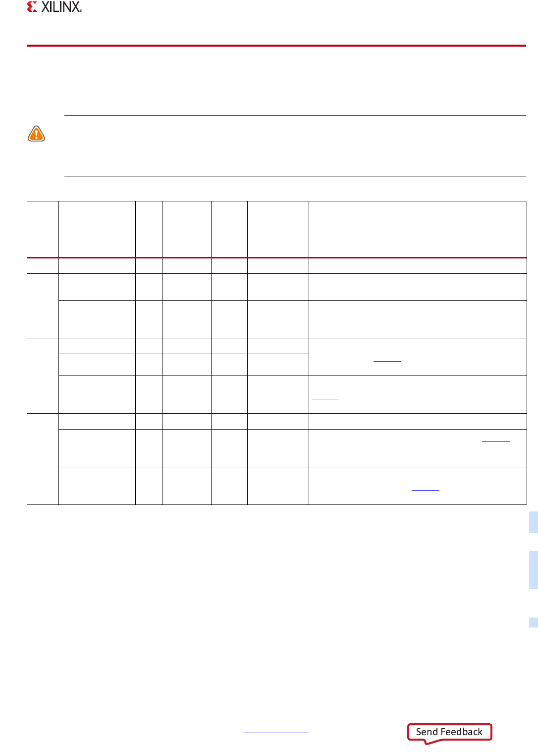
Table 2-2: PS Signal Pins
Group Name Type
Zynq-7000
Family
Pin
Count
(1)
7z007s/
7z010
Device
Pin
Count
Voltage Node Description
Clock PS_CLK I 1 1 V
CCO_MIO0
System reference clock. See Chapter 25, Clocks.
Reset
PS_POR_B I 1 1 V
CCO_MIO0
Power on reset, active low. See Chapter 26, Reset
System.
PS_SRST_B I 1 1 V
CCO_MIO1
Debug system reset, active Low. Forces the system
to enter a reset sequence. See Chapter 26, Reset
System.
MIO
PS_MIO[15:0] I/O 16 16 V
CCO_MIO0
Refer to section 2.5 PS-PL MIO-EMIO Signals and
Interfaces and UG865
, Zynq-7000 AP SoC Package
and Pinout Guide.
PS_MIO[53:16] I/O 38 16 V
CCO_MIO1
PS_MIO_VREF Ref 1 0 V
CCO_MIO1
Voltage reference for RGMII input receivers, refer to
UG933, Zynq-7000 AP SoC PCB Design and Pin
Planning Guide.
DDR
PS_DDR_xxx I/O 73 51 V
CCO_DDR
See Chapter 10, DDR Memory Controller.
PS_DDR_VR[N,P] N/A 2 1 ~
DDR DCI voltage reference pins, refer to UG933,
Zynq-7000 AP SoC PCB Design and Pin Planning
Guide.
PS_DDR_VREF Ref 4 4 ~
Voltage reference for DDR DQ and DQS differential
input receivers, refer to UG933, Zynq-7000 AP SoC
PCB Design and Pin Planning Guide.
Notes:
1. Does not include 7z007s single core and 7z010 dual core CLG225 devices.