
User manual


Table Of Contents
- Zynq-7000 All Programmable SoC
- Table of Contents
- Ch. 1: Introduction
- Ch. 2: Signals, Interfaces, and Pins
- Ch. 3: Application Processing Unit
- Ch. 4: System Addresses
- Ch. 5: Interconnect
- Ch. 6: Boot and Configuration
- Ch. 7: Interrupts
- Ch. 8: Timers
- Ch. 9: DMA Controller
- Introduction
- Functional Description
- DMA Transfers on the AXI Interconnect
- AXI Transaction Considerations
- DMA Manager
- Multi-channel Data FIFO (MFIFO)
- Memory-to-Memory Transfers
- PL Peripheral AXI Transactions
- PL Peripheral Request Interface
- PL Peripheral - Length Managed by PL Peripheral
- PL Peripheral - Length Managed by DMAC
- Events and Interrupts
- Aborts
- Security
- IP Configuration Options
- Programming Guide for DMA Controller
- Programming Guide for DMA Engine
- Programming Restrictions
- System Functions
- I/O Interface
- Ch. 10: DDR Memory Controller
- Introduction
- AXI Memory Port Interface (DDRI)
- DDR Core and Transaction Scheduler (DDRC)
- DDRC Arbitration
- Controller PHY (DDRP)
- Initialization and Calibration
- DDR Clock Initialization
- DDR IOB Impedance Calibration
- DDR IOB Configuration
- DDR Controller Register Programming
- DRAM Reset and Initialization
- DRAM Input Impedance (ODT) Calibration
- DRAM Output Impedance (RON) Calibration
- DRAM Training
- Write Data Eye Adjustment
- Alternatives to Automatic DRAM Training
- DRAM Write Latency Restriction
- Register Overview
- Error Correction Code (ECC)
- Programming Model
- Ch. 11: Static Memory Controller
- Ch. 12: Quad-SPI Flash Controller
- Ch. 13: SD/SDIO Controller
- Ch. 14: General Purpose I/O (GPIO)
- Ch. 15: USB Host, Device, and OTG Controller
- Introduction
- Functional Description
- Programming Overview and Reference
- Device Mode Control
- Device Endpoint Data Structures
- Device Endpoint Packet Operational Model
- Device Endpoint Descriptor Reference
- Programming Guide for Device Controller
- Programming Guide for Device Endpoint Data Structures
- Host Mode Data Structures
- EHCI Implementation
- Host Data Structures Reference
- Programming Guide for Host Controller
- OTG Description and Reference
- System Functions
- I/O Interfaces
- Ch. 16: Gigabit Ethernet Controller
- Ch. 17: SPI Controller
- Ch. 18: CAN Controller
- Ch. 19: UART Controller
- Ch. 20: I2C Controller
- Ch. 21: Programmable Logic Description
- Ch. 22: Programmable Logic Design Guide
- Ch. 23: Programmable Logic Test and Debug
- Ch. 24: Power Management
- Ch. 25: Clocks
- Ch. 26: Reset System
- Ch. 27: JTAG and DAP Subsystem
- Ch. 28: System Test and Debug
- Ch. 29: On-Chip Memory (OCM)
- Ch. 30: XADC Interface
- Ch. 31: PCI Express
- Ch. 32: Device Secure Boot
- Appx. A: Additional Resources
- Appx. B: Register Details
- Overview
- Acronyms
- Module Summary
- AXI_HP Interface (AFI) (axi_hp)
- CAN Controller (can)
- DDR Memory Controller (ddrc)
- CoreSight Cross Trigger Interface (cti)
- Performance Monitor Unit (cortexa9_pmu)
- CoreSight Program Trace Macrocell (ptm)
- Debug Access Port (dap)
- CoreSight Embedded Trace Buffer (etb)
- PL Fabric Trace Monitor (ftm)
- CoreSight Trace Funnel (funnel)
- CoreSight Intstrumentation Trace Macrocell (itm)
- CoreSight Trace Packet Output (tpiu)
- Device Configuration Interface (devcfg)
- DMA Controller (dmac)
- Gigabit Ethernet Controller (GEM)
- General Purpose I/O (gpio)
- Interconnect QoS (qos301)
- NIC301 Address Region Control (nic301_addr_region_ctrl_registers)
- I2C Controller (IIC)
- L2 Cache (L2Cpl310)
- Application Processing Unit (mpcore)
- On-Chip Memory (ocm)
- Quad-SPI Flash Controller (qspi)
- SD Controller (sdio)
- System Level Control Registers (slcr)
- Static Memory Controller (pl353)
- SPI Controller (SPI)
- System Watchdog Timer (swdt)
- Triple Timer Counter (ttc)
- UART Controller (UART)
- USB Controller (usb)
Zynq-7000 AP SoC Technical Reference Manual www.xilinx.com 468
UG585 (v1.11) September 27, 2016
Chapter 15: USB Host, Device, and OTG Controller
15.12.8 Periodic Frame Span Traversal Node (FSTN)
This data structure is to be used only for managing Full- and Low-speed transactions that span a
Host-frame boundary. The HCD must not use an FSTN in the Asynchronous Schedule. An FSTN in the
Asynchronous schedule results in undefined behavior.
FSTN DWord 0: Normal Path Pointer
The first DWord of an FSTN contains a link pointer to the next schedule object. This object can be of
any valid periodic schedule data type.
FSTN DWord 1: Back Path Link Pointer
The second DWord of an FTSN node contains a link pointer to a queue head. If the T-bit in this
pointer is a 0, then this FSTN is a Save-Place indicator. Its TYP field must be set by the HCD to
indicate the target data structure is a queue head. If the T-bit in this pointer is set to a 1, then this
FSTN is the Restore indicator. When the T-bit is a 1, the host controller ignores the TYP field.
Buffer Pointer (pages 3 and 4)
6
and 7
10
and 11
31:12 Buffer Pointer. 4KB aligned pointer to system memory address bits [31:12].
11:0 Reserved.
Table 15-44: USB Host Transfer Overlay Descriptors (Cont’d)
Bits Description
qTD
DWord
QH
DWord
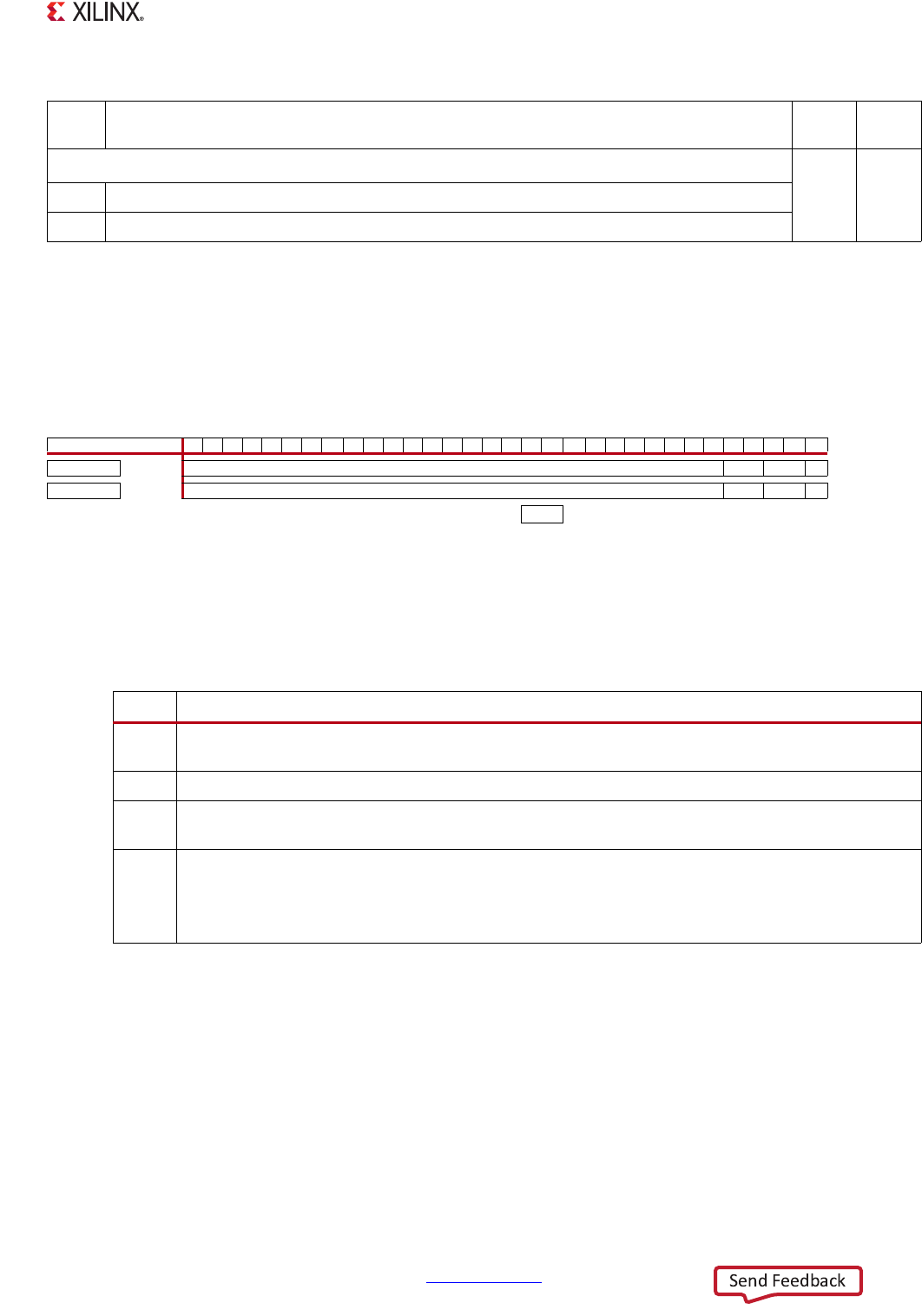
Table 15-45: USB Host Frame Span Traversal Node Descriptor (FSTN) Format
Reference Type 313029282726252423222120191817161514 13 121110 9 8 7 6 5 4 3 2 1 0 DWord
Table 15-46 Normal Path Link Pointer 00 TYP T 0
Table 15-47 Back Path Link Pointer 00 TYP T 1
Host Controller Read-only
Table 15-46: USB Host FSTN DWord: Normal Path Pointer
Bits Description
31:5 Normal Path Link Pointer. Address of the next data object to be processed in the periodic list and
corresponds to memory address bits [31:5], respectively.
4:3 Reserved. Field reserved and should be set to 0.
2:1 Transaction Descriptor Type, TYP. Set to 11 (FSTN type). Refer to section 15.12.2 Transfer Descriptor
Type (TYP) Field for general information.
0 Terminate bit, T.
• 0: Link Pointer field points to a valid system memory offset from CTRLDSSEGMENT and the FSTN
is a Save-Place indicator.
• 1: Link Pointer field is invalid and the FSTN is a Restore indicator.