
User manual


Table Of Contents
- Zynq-7000 All Programmable SoC
- Table of Contents
- Ch. 1: Introduction
- Ch. 2: Signals, Interfaces, and Pins
- Ch. 3: Application Processing Unit
- Ch. 4: System Addresses
- Ch. 5: Interconnect
- Ch. 6: Boot and Configuration
- Ch. 7: Interrupts
- Ch. 8: Timers
- Ch. 9: DMA Controller
- Introduction
- Functional Description
- DMA Transfers on the AXI Interconnect
- AXI Transaction Considerations
- DMA Manager
- Multi-channel Data FIFO (MFIFO)
- Memory-to-Memory Transfers
- PL Peripheral AXI Transactions
- PL Peripheral Request Interface
- PL Peripheral - Length Managed by PL Peripheral
- PL Peripheral - Length Managed by DMAC
- Events and Interrupts
- Aborts
- Security
- IP Configuration Options
- Programming Guide for DMA Controller
- Programming Guide for DMA Engine
- Programming Restrictions
- System Functions
- I/O Interface
- Ch. 10: DDR Memory Controller
- Introduction
- AXI Memory Port Interface (DDRI)
- DDR Core and Transaction Scheduler (DDRC)
- DDRC Arbitration
- Controller PHY (DDRP)
- Initialization and Calibration
- DDR Clock Initialization
- DDR IOB Impedance Calibration
- DDR IOB Configuration
- DDR Controller Register Programming
- DRAM Reset and Initialization
- DRAM Input Impedance (ODT) Calibration
- DRAM Output Impedance (RON) Calibration
- DRAM Training
- Write Data Eye Adjustment
- Alternatives to Automatic DRAM Training
- DRAM Write Latency Restriction
- Register Overview
- Error Correction Code (ECC)
- Programming Model
- Ch. 11: Static Memory Controller
- Ch. 12: Quad-SPI Flash Controller
- Ch. 13: SD/SDIO Controller
- Ch. 14: General Purpose I/O (GPIO)
- Ch. 15: USB Host, Device, and OTG Controller
- Introduction
- Functional Description
- Programming Overview and Reference
- Device Mode Control
- Device Endpoint Data Structures
- Device Endpoint Packet Operational Model
- Device Endpoint Descriptor Reference
- Programming Guide for Device Controller
- Programming Guide for Device Endpoint Data Structures
- Host Mode Data Structures
- EHCI Implementation
- Host Data Structures Reference
- Programming Guide for Host Controller
- OTG Description and Reference
- System Functions
- I/O Interfaces
- Ch. 16: Gigabit Ethernet Controller
- Ch. 17: SPI Controller
- Ch. 18: CAN Controller
- Ch. 19: UART Controller
- Ch. 20: I2C Controller
- Ch. 21: Programmable Logic Description
- Ch. 22: Programmable Logic Design Guide
- Ch. 23: Programmable Logic Test and Debug
- Ch. 24: Power Management
- Ch. 25: Clocks
- Ch. 26: Reset System
- Ch. 27: JTAG and DAP Subsystem
- Ch. 28: System Test and Debug
- Ch. 29: On-Chip Memory (OCM)
- Ch. 30: XADC Interface
- Ch. 31: PCI Express
- Ch. 32: Device Secure Boot
- Appx. A: Additional Resources
- Appx. B: Register Details
- Overview
- Acronyms
- Module Summary
- AXI_HP Interface (AFI) (axi_hp)
- CAN Controller (can)
- DDR Memory Controller (ddrc)
- CoreSight Cross Trigger Interface (cti)
- Performance Monitor Unit (cortexa9_pmu)
- CoreSight Program Trace Macrocell (ptm)
- Debug Access Port (dap)
- CoreSight Embedded Trace Buffer (etb)
- PL Fabric Trace Monitor (ftm)
- CoreSight Trace Funnel (funnel)
- CoreSight Intstrumentation Trace Macrocell (itm)
- CoreSight Trace Packet Output (tpiu)
- Device Configuration Interface (devcfg)
- DMA Controller (dmac)
- Gigabit Ethernet Controller (GEM)
- General Purpose I/O (gpio)
- Interconnect QoS (qos301)
- NIC301 Address Region Control (nic301_addr_region_ctrl_registers)
- I2C Controller (IIC)
- L2 Cache (L2Cpl310)
- Application Processing Unit (mpcore)
- On-Chip Memory (ocm)
- Quad-SPI Flash Controller (qspi)
- SD Controller (sdio)
- System Level Control Registers (slcr)
- Static Memory Controller (pl353)
- SPI Controller (SPI)
- System Watchdog Timer (swdt)
- Triple Timer Counter (ttc)
- UART Controller (UART)
- USB Controller (usb)
Zynq-7000 AP SoC Technical Reference Manual www.xilinx.com 489
UG585 (v1.11) September 27, 2016
Chapter 16: Gigabit Ethernet Controller
DMA Controller
The DMA uses separate transmit and receive lists of buffer descriptors, with each descriptor
describing a buffer area in memory. This allows Ethernet packets to be broken up and scattered
around the AHB memory space.
The DMA controller performs four types of operation on the AHB bus. In order of priority these are:
• Receive buffer manager write/read
• Transmit buffer manager write/read
• Receive data DMA write
• Transmit data DMA read
Transfer size is set to 32-bit words using the AHB bus width select bits in the Network Configuration
register, and burst size may be programmed to single access or bursts of 4, 8, or 16 words using the
DMA Configuration register.
Rx Buffers
Received frames, optionally including FCS, are written to receive AHB buffers stored in memory. The
start location for each receive AHB buffer is stored in memory in a list of receive buffer descriptors
at an address location pointed to by the receive-buffer queue pointer. The base address for the
receive-buffer queue pointer is configured in software using the Receive Buffer Queue Base Address
register.
Each list entry consists of two words. The first is the address of the receive AHB buffer and the
second the receive status. If the length of a receive frame exceeds the AHB buffer length, the status
word for the used buffer is written with zeroes except for the start of frame bit, which is always set for
the first buffer in a frame. Bit zero of the address field is written to 1 to show that the buffer has been
used. The receive-buffer manager then reads the location of the next receive AHB buffer and fills that
with the next part of the received frame data. AHB buffers are filled until the frame is complete and
the final buffer descriptor status word contains the complete frame status. Refer to Table 16-2 for
details of the receive buffer descriptor list.
Each receive AHB buffer start location is a word address. The start of the first AHB buffer in a frame
can be offset by up to three bytes depending on the value written to bits [14] and [15] of the Network
Configuration register. If the start location of the AHB buffer is offset the available length of the first
AHB buffer is reduced by the corresponding number of bytes.
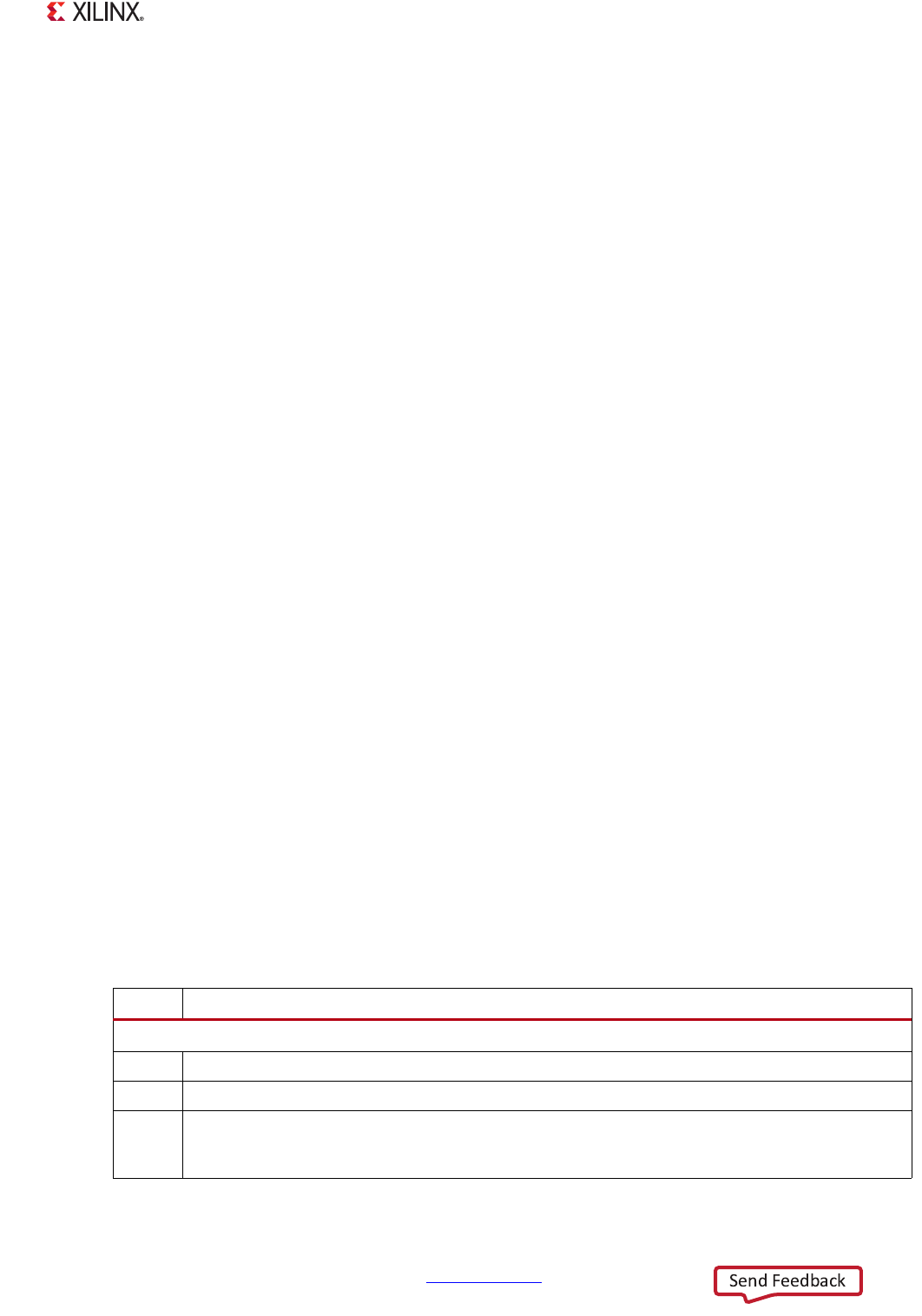
Table 16-2: Rx Buffer Descriptor Entry
Bit Function
Word 0
31:2 Address of beginning of buffer.
1 Wrap - marks last descriptor in receive buffer descriptor list.
0 Ownership - needs to be zero for the controller to write data to the receive buffer. The controller
sets this to 1 once it has successfully written a frame to memory. Software must clear this bit before
the buffer can be used again.