
User manual


Table Of Contents
- Zynq-7000 All Programmable SoC
- Table of Contents
- Ch. 1: Introduction
- Ch. 2: Signals, Interfaces, and Pins
- Ch. 3: Application Processing Unit
- Ch. 4: System Addresses
- Ch. 5: Interconnect
- Ch. 6: Boot and Configuration
- Ch. 7: Interrupts
- Ch. 8: Timers
- Ch. 9: DMA Controller
- Introduction
- Functional Description
- DMA Transfers on the AXI Interconnect
- AXI Transaction Considerations
- DMA Manager
- Multi-channel Data FIFO (MFIFO)
- Memory-to-Memory Transfers
- PL Peripheral AXI Transactions
- PL Peripheral Request Interface
- PL Peripheral - Length Managed by PL Peripheral
- PL Peripheral - Length Managed by DMAC
- Events and Interrupts
- Aborts
- Security
- IP Configuration Options
- Programming Guide for DMA Controller
- Programming Guide for DMA Engine
- Programming Restrictions
- System Functions
- I/O Interface
- Ch. 10: DDR Memory Controller
- Introduction
- AXI Memory Port Interface (DDRI)
- DDR Core and Transaction Scheduler (DDRC)
- DDRC Arbitration
- Controller PHY (DDRP)
- Initialization and Calibration
- DDR Clock Initialization
- DDR IOB Impedance Calibration
- DDR IOB Configuration
- DDR Controller Register Programming
- DRAM Reset and Initialization
- DRAM Input Impedance (ODT) Calibration
- DRAM Output Impedance (RON) Calibration
- DRAM Training
- Write Data Eye Adjustment
- Alternatives to Automatic DRAM Training
- DRAM Write Latency Restriction
- Register Overview
- Error Correction Code (ECC)
- Programming Model
- Ch. 11: Static Memory Controller
- Ch. 12: Quad-SPI Flash Controller
- Ch. 13: SD/SDIO Controller
- Ch. 14: General Purpose I/O (GPIO)
- Ch. 15: USB Host, Device, and OTG Controller
- Introduction
- Functional Description
- Programming Overview and Reference
- Device Mode Control
- Device Endpoint Data Structures
- Device Endpoint Packet Operational Model
- Device Endpoint Descriptor Reference
- Programming Guide for Device Controller
- Programming Guide for Device Endpoint Data Structures
- Host Mode Data Structures
- EHCI Implementation
- Host Data Structures Reference
- Programming Guide for Host Controller
- OTG Description and Reference
- System Functions
- I/O Interfaces
- Ch. 16: Gigabit Ethernet Controller
- Ch. 17: SPI Controller
- Ch. 18: CAN Controller
- Ch. 19: UART Controller
- Ch. 20: I2C Controller
- Ch. 21: Programmable Logic Description
- Ch. 22: Programmable Logic Design Guide
- Ch. 23: Programmable Logic Test and Debug
- Ch. 24: Power Management
- Ch. 25: Clocks
- Ch. 26: Reset System
- Ch. 27: JTAG and DAP Subsystem
- Ch. 28: System Test and Debug
- Ch. 29: On-Chip Memory (OCM)
- Ch. 30: XADC Interface
- Ch. 31: PCI Express
- Ch. 32: Device Secure Boot
- Appx. A: Additional Resources
- Appx. B: Register Details
- Overview
- Acronyms
- Module Summary
- AXI_HP Interface (AFI) (axi_hp)
- CAN Controller (can)
- DDR Memory Controller (ddrc)
- CoreSight Cross Trigger Interface (cti)
- Performance Monitor Unit (cortexa9_pmu)
- CoreSight Program Trace Macrocell (ptm)
- Debug Access Port (dap)
- CoreSight Embedded Trace Buffer (etb)
- PL Fabric Trace Monitor (ftm)
- CoreSight Trace Funnel (funnel)
- CoreSight Intstrumentation Trace Macrocell (itm)
- CoreSight Trace Packet Output (tpiu)
- Device Configuration Interface (devcfg)
- DMA Controller (dmac)
- Gigabit Ethernet Controller (GEM)
- General Purpose I/O (gpio)
- Interconnect QoS (qos301)
- NIC301 Address Region Control (nic301_addr_region_ctrl_registers)
- I2C Controller (IIC)
- L2 Cache (L2Cpl310)
- Application Processing Unit (mpcore)
- On-Chip Memory (ocm)
- Quad-SPI Flash Controller (qspi)
- SD Controller (sdio)
- System Level Control Registers (slcr)
- Static Memory Controller (pl353)
- SPI Controller (SPI)
- System Watchdog Timer (swdt)
- Triple Timer Counter (ttc)
- UART Controller (UART)
- USB Controller (usb)
Zynq-7000 AP SoC Technical Reference Manual www.xilinx.com 512
UG585 (v1.11) September 27, 2016
Chapter 16: Gigabit Ethernet Controller
To create this list of buffers:
1. Allocate a number (N) of buffers of X bytes in system memory, where X is the DMA buffer length
programmed in the DMA Configuration register.
Example: This controller assumes that the maximum size of an Ethernet packet without jumbo
frame support can reach up to 1,536 bytes. So allocate N number of buffers each with a size of
1,536 bytes in system memory. The buffers typically need to be aligned to cache-line boundaries
to improve performance. Typical values of N can be 64 or 128.
2. Each buffer descriptor is of 8 bytes length. Hence allocate an area of 8N bytes for the receive
buffer descriptor list in system memory. This creates N entries in this list.
Note: A single cache line for the Zynq-7000 AP SoC is 32 bytes and can contain 4 buffer
descriptors. This means flushing or invalidating a single buffer descriptor entry in the cache
memory results in flushing or invalidation of a cache line which in turn affects the adjacent buffer
descriptors. This can result in undesirable behavior. It is typical to allocate the buffer descriptor
list in an un-cached memory region.
3. Mark all entries in this list as owned by controller. Set bit 0 of word 0 of each buffer descriptor to
0.
4. Mark the last descriptor in the buffer descriptor list with the wrap bit (bit 1 in word 0) set.
5. Write the base address of receive buffer descriptor list to controller register gem.rx_qbar.
6. Fill the addresses of the allocated buffers in the buffer descriptors (bits 31-2, Word 0).
7. Write the base address of this buffer descriptor list to the gem.rx_qbar register.
Transmit Buffer Descriptor List
The data to be transmitted is read from buffers present in system memory. These buffers are listed
in the transmit buffer queue. Refer to section 16.2.5 DMA Block and Table 16-2, page 489 for more
information on implementation and structure of the Tx buffer descriptor.
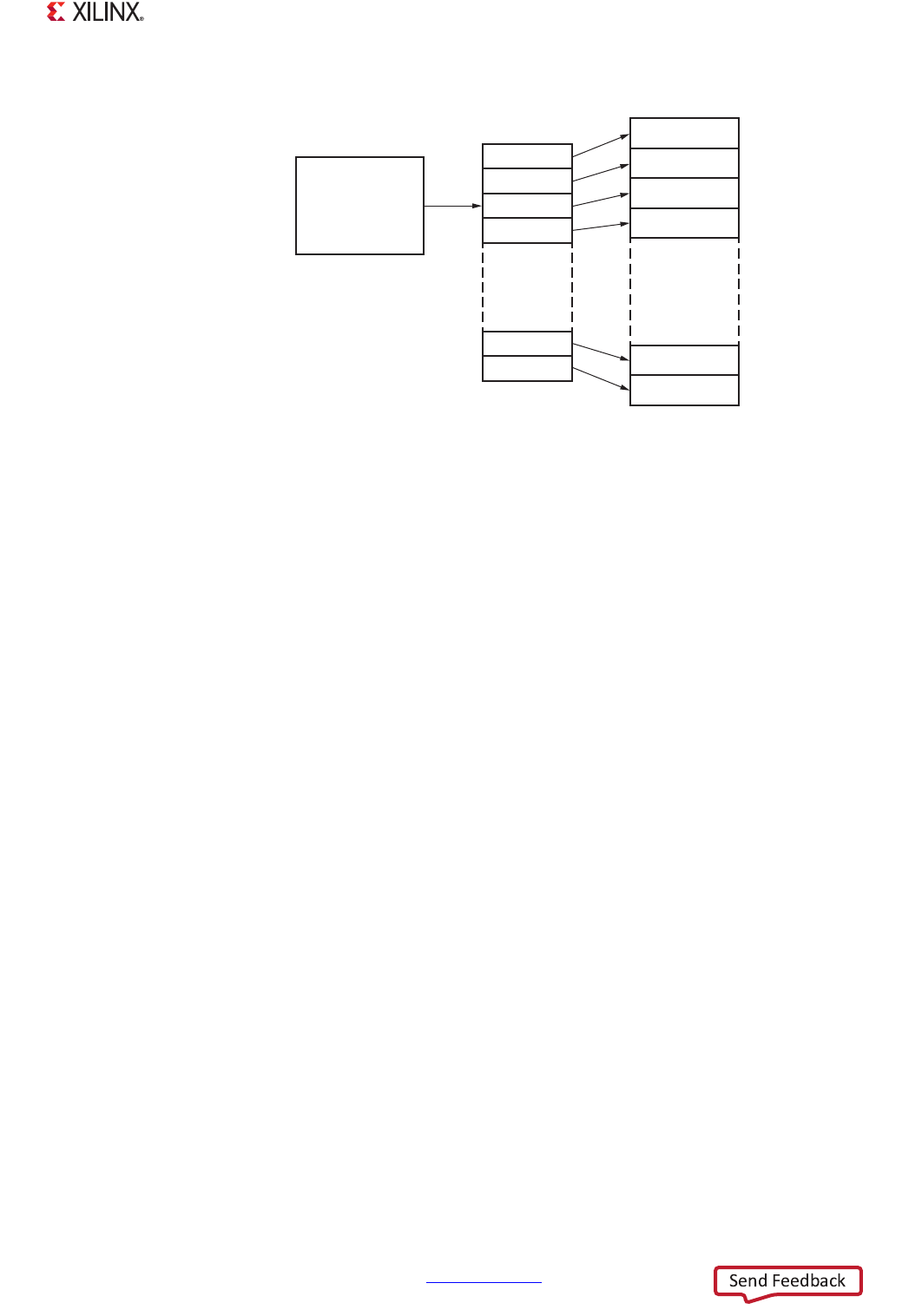
X-Ref Target - Figure 16-4
Figure 16-4: Rx Buffer Queue Structure
UG585_c16_04_022712
Rx Buffer
Queue Pointer
MAC Register
Rx
Descripter List
List in Main
Memory
Buffer in Main
Memory
Rx Buffers