
User manual


Table Of Contents
- Zynq-7000 All Programmable SoC
- Table of Contents
- Ch. 1: Introduction
- Ch. 2: Signals, Interfaces, and Pins
- Ch. 3: Application Processing Unit
- Ch. 4: System Addresses
- Ch. 5: Interconnect
- Ch. 6: Boot and Configuration
- Ch. 7: Interrupts
- Ch. 8: Timers
- Ch. 9: DMA Controller
- Introduction
- Functional Description
- DMA Transfers on the AXI Interconnect
- AXI Transaction Considerations
- DMA Manager
- Multi-channel Data FIFO (MFIFO)
- Memory-to-Memory Transfers
- PL Peripheral AXI Transactions
- PL Peripheral Request Interface
- PL Peripheral - Length Managed by PL Peripheral
- PL Peripheral - Length Managed by DMAC
- Events and Interrupts
- Aborts
- Security
- IP Configuration Options
- Programming Guide for DMA Controller
- Programming Guide for DMA Engine
- Programming Restrictions
- System Functions
- I/O Interface
- Ch. 10: DDR Memory Controller
- Introduction
- AXI Memory Port Interface (DDRI)
- DDR Core and Transaction Scheduler (DDRC)
- DDRC Arbitration
- Controller PHY (DDRP)
- Initialization and Calibration
- DDR Clock Initialization
- DDR IOB Impedance Calibration
- DDR IOB Configuration
- DDR Controller Register Programming
- DRAM Reset and Initialization
- DRAM Input Impedance (ODT) Calibration
- DRAM Output Impedance (RON) Calibration
- DRAM Training
- Write Data Eye Adjustment
- Alternatives to Automatic DRAM Training
- DRAM Write Latency Restriction
- Register Overview
- Error Correction Code (ECC)
- Programming Model
- Ch. 11: Static Memory Controller
- Ch. 12: Quad-SPI Flash Controller
- Ch. 13: SD/SDIO Controller
- Ch. 14: General Purpose I/O (GPIO)
- Ch. 15: USB Host, Device, and OTG Controller
- Introduction
- Functional Description
- Programming Overview and Reference
- Device Mode Control
- Device Endpoint Data Structures
- Device Endpoint Packet Operational Model
- Device Endpoint Descriptor Reference
- Programming Guide for Device Controller
- Programming Guide for Device Endpoint Data Structures
- Host Mode Data Structures
- EHCI Implementation
- Host Data Structures Reference
- Programming Guide for Host Controller
- OTG Description and Reference
- System Functions
- I/O Interfaces
- Ch. 16: Gigabit Ethernet Controller
- Ch. 17: SPI Controller
- Ch. 18: CAN Controller
- Ch. 19: UART Controller
- Ch. 20: I2C Controller
- Ch. 21: Programmable Logic Description
- Ch. 22: Programmable Logic Design Guide
- Ch. 23: Programmable Logic Test and Debug
- Ch. 24: Power Management
- Ch. 25: Clocks
- Ch. 26: Reset System
- Ch. 27: JTAG and DAP Subsystem
- Ch. 28: System Test and Debug
- Ch. 29: On-Chip Memory (OCM)
- Ch. 30: XADC Interface
- Ch. 31: PCI Express
- Ch. 32: Device Secure Boot
- Appx. A: Additional Resources
- Appx. B: Register Details
- Overview
- Acronyms
- Module Summary
- AXI_HP Interface (AFI) (axi_hp)
- CAN Controller (can)
- DDR Memory Controller (ddrc)
- CoreSight Cross Trigger Interface (cti)
- Performance Monitor Unit (cortexa9_pmu)
- CoreSight Program Trace Macrocell (ptm)
- Debug Access Port (dap)
- CoreSight Embedded Trace Buffer (etb)
- PL Fabric Trace Monitor (ftm)
- CoreSight Trace Funnel (funnel)
- CoreSight Intstrumentation Trace Macrocell (itm)
- CoreSight Trace Packet Output (tpiu)
- Device Configuration Interface (devcfg)
- DMA Controller (dmac)
- Gigabit Ethernet Controller (GEM)
- General Purpose I/O (gpio)
- Interconnect QoS (qos301)
- NIC301 Address Region Control (nic301_addr_region_ctrl_registers)
- I2C Controller (IIC)
- L2 Cache (L2Cpl310)
- Application Processing Unit (mpcore)
- On-Chip Memory (ocm)
- Quad-SPI Flash Controller (qspi)
- SD Controller (sdio)
- System Level Control Registers (slcr)
- Static Memory Controller (pl353)
- SPI Controller (SPI)
- System Watchdog Timer (swdt)
- Triple Timer Counter (ttc)
- UART Controller (UART)
- USB Controller (usb)
Zynq-7000 AP SoC Technical Reference Manual www.xilinx.com 53
UG585 (v1.11) September 27, 2016
Chapter 2: Signals, Interfaces, and Pins
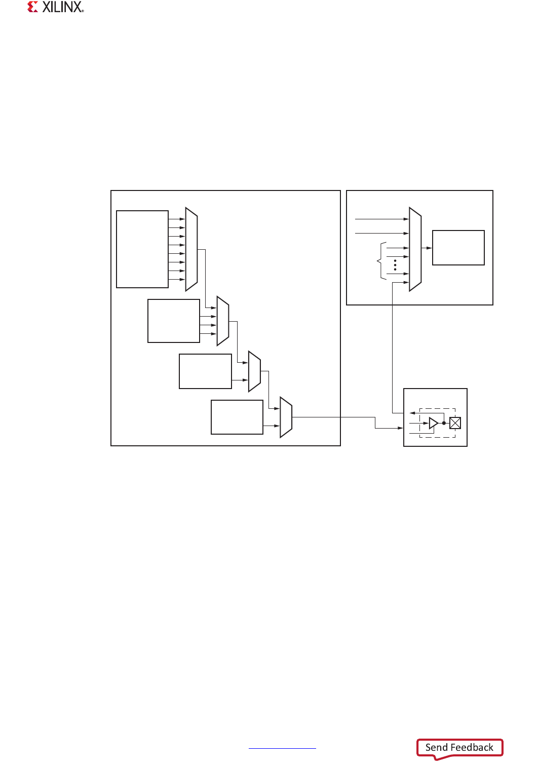
2.5.5 MIO Signal Routing
Signal routing through the MIO is controlled by the MIO_PIN_[53:0] configuration registers located
in the slcr registers set. The MIO multiplexes and de-multiplexes the various input and output signals
to the MIO pins using four stages of multiplexing, as shown in Figure 2-4. The high-speed data
signals (such as RGMII for Gigabit Ethernet and ULPI for USB) are routed through only one
multiplexer stage. The slower signals (such as the UART and I2C ports) are routed through all four
multiplexer stages. The routing for each MIO pin is independently controlled by multiple bit fields in
each MIO_PIN register.
Any of the MIO pins can be programmed to be an external CAN controller reference clock using the
CAN_MIOCLK_CTRL register.
2.5.6 Default Logic Levels
The inputs to the I/O peripherals are driven with default values when another source is not routed to
either the MIO or the EMIO. If an input is routed to EMIO, but the PL is powered down, then the same
default value is driven to the I/O peripheral. (See Figure 2-5.)
For MIO-only signals, the default signal input is driven when the MIO multiplexer does not route the
signal to an MIO pin.
For MIO-EMIO signals, the default signal input is driven when the MIO multiplexer does not route the
signal to an MIO pin (the signal defaults to the EMIO interface) and when the signal is programmed
to be routed through the EMIO, but the PL either does not drive the signal (not configured) or is not
able to drive it (powered down).
X-Ref Target - Figure 2-4
Figure 2-4: MIO Signal Routing
UG585_c2_04_042312
Controller
Outputs
Outputs
from
Controllers
Notice: Not all mux
inputs are populated
with controller outputs.
Inputs to
Controllers
Level 3 Muxing
Level 2 Muxing
0
1
2
3
4
5
6
7
Controller
Outputs
0
Input Tie-Offs
EMIO
Other
MIO
Pins
1
2
3
Level 1 Muxing
Controller
Output
Controller
Input
0
1
Level 0 Muxing
Controller
Output
MIO Pin
0
1
To Program Muxing
Levels, refer to the
select fields in Registers
MIO_PIN_[53:00]