
User manual


Table Of Contents
- Zynq-7000 All Programmable SoC
- Table of Contents
- Ch. 1: Introduction
- Ch. 2: Signals, Interfaces, and Pins
- Ch. 3: Application Processing Unit
- Ch. 4: System Addresses
- Ch. 5: Interconnect
- Ch. 6: Boot and Configuration
- Ch. 7: Interrupts
- Ch. 8: Timers
- Ch. 9: DMA Controller
- Introduction
- Functional Description
- DMA Transfers on the AXI Interconnect
- AXI Transaction Considerations
- DMA Manager
- Multi-channel Data FIFO (MFIFO)
- Memory-to-Memory Transfers
- PL Peripheral AXI Transactions
- PL Peripheral Request Interface
- PL Peripheral - Length Managed by PL Peripheral
- PL Peripheral - Length Managed by DMAC
- Events and Interrupts
- Aborts
- Security
- IP Configuration Options
- Programming Guide for DMA Controller
- Programming Guide for DMA Engine
- Programming Restrictions
- System Functions
- I/O Interface
- Ch. 10: DDR Memory Controller
- Introduction
- AXI Memory Port Interface (DDRI)
- DDR Core and Transaction Scheduler (DDRC)
- DDRC Arbitration
- Controller PHY (DDRP)
- Initialization and Calibration
- DDR Clock Initialization
- DDR IOB Impedance Calibration
- DDR IOB Configuration
- DDR Controller Register Programming
- DRAM Reset and Initialization
- DRAM Input Impedance (ODT) Calibration
- DRAM Output Impedance (RON) Calibration
- DRAM Training
- Write Data Eye Adjustment
- Alternatives to Automatic DRAM Training
- DRAM Write Latency Restriction
- Register Overview
- Error Correction Code (ECC)
- Programming Model
- Ch. 11: Static Memory Controller
- Ch. 12: Quad-SPI Flash Controller
- Ch. 13: SD/SDIO Controller
- Ch. 14: General Purpose I/O (GPIO)
- Ch. 15: USB Host, Device, and OTG Controller
- Introduction
- Functional Description
- Programming Overview and Reference
- Device Mode Control
- Device Endpoint Data Structures
- Device Endpoint Packet Operational Model
- Device Endpoint Descriptor Reference
- Programming Guide for Device Controller
- Programming Guide for Device Endpoint Data Structures
- Host Mode Data Structures
- EHCI Implementation
- Host Data Structures Reference
- Programming Guide for Host Controller
- OTG Description and Reference
- System Functions
- I/O Interfaces
- Ch. 16: Gigabit Ethernet Controller
- Ch. 17: SPI Controller
- Ch. 18: CAN Controller
- Ch. 19: UART Controller
- Ch. 20: I2C Controller
- Ch. 21: Programmable Logic Description
- Ch. 22: Programmable Logic Design Guide
- Ch. 23: Programmable Logic Test and Debug
- Ch. 24: Power Management
- Ch. 25: Clocks
- Ch. 26: Reset System
- Ch. 27: JTAG and DAP Subsystem
- Ch. 28: System Test and Debug
- Ch. 29: On-Chip Memory (OCM)
- Ch. 30: XADC Interface
- Ch. 31: PCI Express
- Ch. 32: Device Secure Boot
- Appx. A: Additional Resources
- Appx. B: Register Details
- Overview
- Acronyms
- Module Summary
- AXI_HP Interface (AFI) (axi_hp)
- CAN Controller (can)
- DDR Memory Controller (ddrc)
- CoreSight Cross Trigger Interface (cti)
- Performance Monitor Unit (cortexa9_pmu)
- CoreSight Program Trace Macrocell (ptm)
- Debug Access Port (dap)
- CoreSight Embedded Trace Buffer (etb)
- PL Fabric Trace Monitor (ftm)
- CoreSight Trace Funnel (funnel)
- CoreSight Intstrumentation Trace Macrocell (itm)
- CoreSight Trace Packet Output (tpiu)
- Device Configuration Interface (devcfg)
- DMA Controller (dmac)
- Gigabit Ethernet Controller (GEM)
- General Purpose I/O (gpio)
- Interconnect QoS (qos301)
- NIC301 Address Region Control (nic301_addr_region_ctrl_registers)
- I2C Controller (IIC)
- L2 Cache (L2Cpl310)
- Application Processing Unit (mpcore)
- On-Chip Memory (ocm)
- Quad-SPI Flash Controller (qspi)
- SD Controller (sdio)
- System Level Control Registers (slcr)
- Static Memory Controller (pl353)
- SPI Controller (SPI)
- System Watchdog Timer (swdt)
- Triple Timer Counter (ttc)
- UART Controller (UART)
- USB Controller (usb)
Zynq-7000 AP SoC Technical Reference Manual www.xilinx.com 56
UG585 (v1.11) September 27, 2016
Chapter 2: Signals, Interfaces, and Pins
Note: The PL level shifters must be enabled via the slcr.LVL_SHFTR_EN register before PL logic
communication can occur, refer to section 2.7.1 Clocks and Resets.
2.7.1 Clocks and Resets
Clocks
The PS clock module provides four frequency-programmable clocks (FCLKs) to the PL that are
physically spread out along the PS–PL boundary. The clocks can also be individually controlled. The
FCLK clocks can be routed to PL clock buffers to serve as a frequency source.
Note: There is no guaranteed timing relationship between any of the four PL clocks and between
any of the other PS-PL signals. Each clock is independently programmed and operated. The
FCLKCLKTRIGN[3:0] signals are currently not supported. They must be tied to ground in the PL. The
FCLK clocks are described in
Chapter 25, Clocks.
Resets
The PS reset subsystem provides four programmable reset signals to the PL. The reset signals are
controlled by writing to the slcr.FPGA_RST_CTRL SLCR[FPGA[3:0]_OUT_RST] bit fields. The resets are
independently programmed and are completely independent of the PL clocks and all other PS-PL
signals. The PS reset subsystem is described in
Chapter 26, Reset System.
The PL clocks and resets are summarized in Table 2-8.
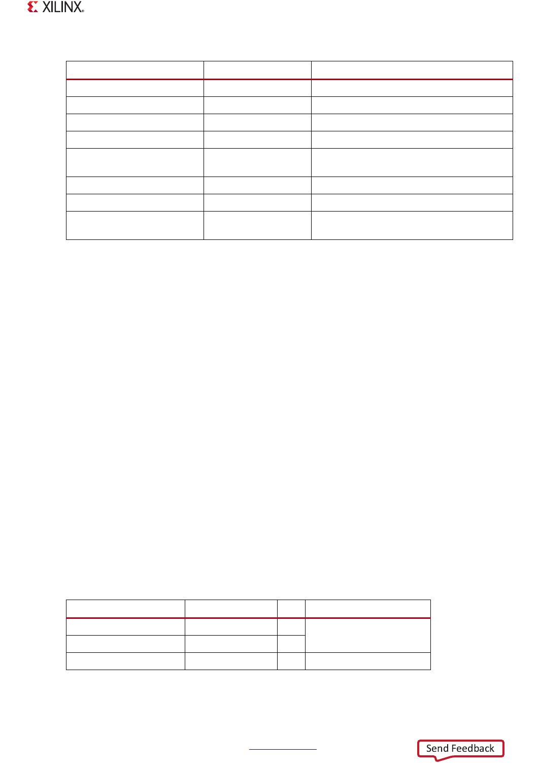
Table 2-7: PS-PL Signal Groups
PS-PL Signal Group Signal Name Reference
PL clocks and resets FCLKx 2.7.1 Clocks and Resets
PL interrupts to PS IRQF2Px 2.7.2 Interrupt Signals
IOP interrupts to PL IRQP2Fx 2.7.2 Interrupt Signals
Events EVENTx 2.7.3 Event Signals
IdleAXI, DDR ARB, SRAM
interrupt, FPGA
FPGA, DDR, EMIO 2.7.4 Idle AXI, DDR Urgent/Arb, SRAM
Interrupt Signals
DMA controller DMACx 2.7.5 DMA Req/Ack Signals
EMIO signals EMIOx Table 2-3
USB port indicator and power
control
EMIOUSBx 15.16.3 MIO-EMIO Signals
Table 2-8: PL Clock and Reset Signals
Type PL Signal Name I/O Reference
PL Clocks FCLKCLK[3:0] O
Chapter 25, Clocks
PL Clock Throttle Control FCLKCLKTRIG [3:0] I
PL Resets FCLKRESETN [3:0] O Chapter 26, Reset System