
User manual


Table Of Contents
- Zynq-7000 All Programmable SoC
- Table of Contents
- Ch. 1: Introduction
- Ch. 2: Signals, Interfaces, and Pins
- Ch. 3: Application Processing Unit
- Ch. 4: System Addresses
- Ch. 5: Interconnect
- Ch. 6: Boot and Configuration
- Ch. 7: Interrupts
- Ch. 8: Timers
- Ch. 9: DMA Controller
- Introduction
- Functional Description
- DMA Transfers on the AXI Interconnect
- AXI Transaction Considerations
- DMA Manager
- Multi-channel Data FIFO (MFIFO)
- Memory-to-Memory Transfers
- PL Peripheral AXI Transactions
- PL Peripheral Request Interface
- PL Peripheral - Length Managed by PL Peripheral
- PL Peripheral - Length Managed by DMAC
- Events and Interrupts
- Aborts
- Security
- IP Configuration Options
- Programming Guide for DMA Controller
- Programming Guide for DMA Engine
- Programming Restrictions
- System Functions
- I/O Interface
- Ch. 10: DDR Memory Controller
- Introduction
- AXI Memory Port Interface (DDRI)
- DDR Core and Transaction Scheduler (DDRC)
- DDRC Arbitration
- Controller PHY (DDRP)
- Initialization and Calibration
- DDR Clock Initialization
- DDR IOB Impedance Calibration
- DDR IOB Configuration
- DDR Controller Register Programming
- DRAM Reset and Initialization
- DRAM Input Impedance (ODT) Calibration
- DRAM Output Impedance (RON) Calibration
- DRAM Training
- Write Data Eye Adjustment
- Alternatives to Automatic DRAM Training
- DRAM Write Latency Restriction
- Register Overview
- Error Correction Code (ECC)
- Programming Model
- Ch. 11: Static Memory Controller
- Ch. 12: Quad-SPI Flash Controller
- Ch. 13: SD/SDIO Controller
- Ch. 14: General Purpose I/O (GPIO)
- Ch. 15: USB Host, Device, and OTG Controller
- Introduction
- Functional Description
- Programming Overview and Reference
- Device Mode Control
- Device Endpoint Data Structures
- Device Endpoint Packet Operational Model
- Device Endpoint Descriptor Reference
- Programming Guide for Device Controller
- Programming Guide for Device Endpoint Data Structures
- Host Mode Data Structures
- EHCI Implementation
- Host Data Structures Reference
- Programming Guide for Host Controller
- OTG Description and Reference
- System Functions
- I/O Interfaces
- Ch. 16: Gigabit Ethernet Controller
- Ch. 17: SPI Controller
- Ch. 18: CAN Controller
- Ch. 19: UART Controller
- Ch. 20: I2C Controller
- Ch. 21: Programmable Logic Description
- Ch. 22: Programmable Logic Design Guide
- Ch. 23: Programmable Logic Test and Debug
- Ch. 24: Power Management
- Ch. 25: Clocks
- Ch. 26: Reset System
- Ch. 27: JTAG and DAP Subsystem
- Ch. 28: System Test and Debug
- Ch. 29: On-Chip Memory (OCM)
- Ch. 30: XADC Interface
- Ch. 31: PCI Express
- Ch. 32: Device Secure Boot
- Appx. A: Additional Resources
- Appx. B: Register Details
- Overview
- Acronyms
- Module Summary
- AXI_HP Interface (AFI) (axi_hp)
- CAN Controller (can)
- DDR Memory Controller (ddrc)
- CoreSight Cross Trigger Interface (cti)
- Performance Monitor Unit (cortexa9_pmu)
- CoreSight Program Trace Macrocell (ptm)
- Debug Access Port (dap)
- CoreSight Embedded Trace Buffer (etb)
- PL Fabric Trace Monitor (ftm)
- CoreSight Trace Funnel (funnel)
- CoreSight Intstrumentation Trace Macrocell (itm)
- CoreSight Trace Packet Output (tpiu)
- Device Configuration Interface (devcfg)
- DMA Controller (dmac)
- Gigabit Ethernet Controller (GEM)
- General Purpose I/O (gpio)
- Interconnect QoS (qos301)
- NIC301 Address Region Control (nic301_addr_region_ctrl_registers)
- I2C Controller (IIC)
- L2 Cache (L2Cpl310)
- Application Processing Unit (mpcore)
- On-Chip Memory (ocm)
- Quad-SPI Flash Controller (qspi)
- SD Controller (sdio)
- System Level Control Registers (slcr)
- Static Memory Controller (pl353)
- SPI Controller (SPI)
- System Watchdog Timer (swdt)
- Triple Timer Counter (ttc)
- UART Controller (UART)
- USB Controller (usb)
Zynq-7000 AP SoC Technical Reference Manual www.xilinx.com 564
UG585 (v1.11) September 27, 2016
Chapter 18: CAN Controller
Reads
Data starts at byte 0 and continues for the number of counts in DLC. Software should read both data
words, but the only valid bytes are determined by DLC.
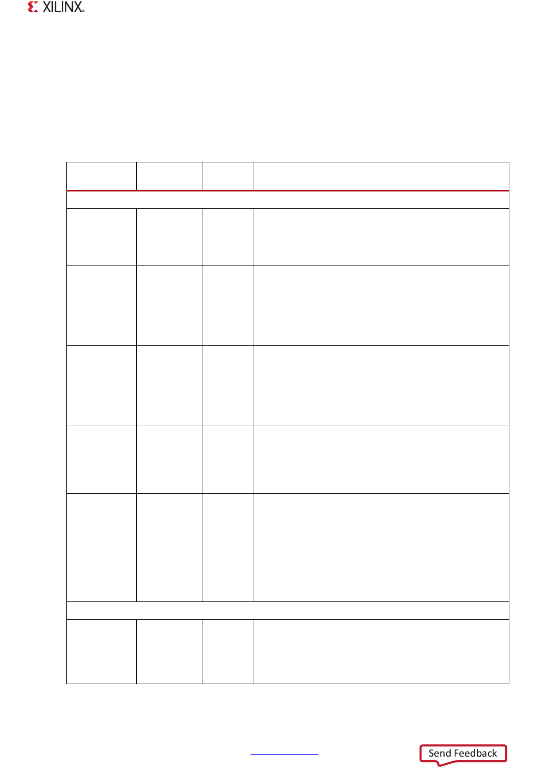
Table 18-3 provides bit descriptions for the identifier word bits, the DLC word bits, and data word 1
and data word 2 bits.
Table 18-3: CAN Message Word Register Bit Fields
Bits Name
Default
Value
Description
Identifier Word
31:21 ID[28:18] 0
Standard Message ID
The identifier portion for a standard frame is 11 bits.
These bits indicate the standard frame ID.
This field is valid for both standard and extended frames.
20 SRR/RTR 0
Substitute Remote Transmission Request
This bit differentiates between data frames and remote
frames. Valid only for standard frames. For extended
frames this bit is 1.
1: Indicates that the message frame is a Remote Frame.
0: Indicates that the message frame is a Data Frame.
19 IDE 0
Identifier Extension
This bit differentiates between frames using the Standard
Identifier and those using the Extended Identifier. Valid
for both Standard and Extended Frames.
1: Indicates the use of an extended message identifier.
0: Indicates the use of a standard message identifier.
18:1 ID[17:0] 0
Extended Message ID
This field indicates the extended identifier. Valid only for
extended frames.
For standard frames, reads from this field return 0s.
For Standard frames, writes to this field should be 0s.
0RTR0
Remote Transmission Request
This bit differentiates between data frames and remote
frames.
Valid only for extended frames.
1: Indicates the message object is a remote frame.
0: Indicates the message object is a data frame.
For standard frames, reads from this bit returns 0.
For standard frames, writes to this bit should be 0.
DLC Word
31-28 DLC 0
Data Length Code
This is the data length portion of the control field of the
CAN frame. This indicates the number valid data bytes (0
to 8) that are in the Data Word 1 and Data Word 2
registers.