
User manual


Table Of Contents
- Zynq-7000 All Programmable SoC
- Table of Contents
- Ch. 1: Introduction
- Ch. 2: Signals, Interfaces, and Pins
- Ch. 3: Application Processing Unit
- Ch. 4: System Addresses
- Ch. 5: Interconnect
- Ch. 6: Boot and Configuration
- Ch. 7: Interrupts
- Ch. 8: Timers
- Ch. 9: DMA Controller
- Introduction
- Functional Description
- DMA Transfers on the AXI Interconnect
- AXI Transaction Considerations
- DMA Manager
- Multi-channel Data FIFO (MFIFO)
- Memory-to-Memory Transfers
- PL Peripheral AXI Transactions
- PL Peripheral Request Interface
- PL Peripheral - Length Managed by PL Peripheral
- PL Peripheral - Length Managed by DMAC
- Events and Interrupts
- Aborts
- Security
- IP Configuration Options
- Programming Guide for DMA Controller
- Programming Guide for DMA Engine
- Programming Restrictions
- System Functions
- I/O Interface
- Ch. 10: DDR Memory Controller
- Introduction
- AXI Memory Port Interface (DDRI)
- DDR Core and Transaction Scheduler (DDRC)
- DDRC Arbitration
- Controller PHY (DDRP)
- Initialization and Calibration
- DDR Clock Initialization
- DDR IOB Impedance Calibration
- DDR IOB Configuration
- DDR Controller Register Programming
- DRAM Reset and Initialization
- DRAM Input Impedance (ODT) Calibration
- DRAM Output Impedance (RON) Calibration
- DRAM Training
- Write Data Eye Adjustment
- Alternatives to Automatic DRAM Training
- DRAM Write Latency Restriction
- Register Overview
- Error Correction Code (ECC)
- Programming Model
- Ch. 11: Static Memory Controller
- Ch. 12: Quad-SPI Flash Controller
- Ch. 13: SD/SDIO Controller
- Ch. 14: General Purpose I/O (GPIO)
- Ch. 15: USB Host, Device, and OTG Controller
- Introduction
- Functional Description
- Programming Overview and Reference
- Device Mode Control
- Device Endpoint Data Structures
- Device Endpoint Packet Operational Model
- Device Endpoint Descriptor Reference
- Programming Guide for Device Controller
- Programming Guide for Device Endpoint Data Structures
- Host Mode Data Structures
- EHCI Implementation
- Host Data Structures Reference
- Programming Guide for Host Controller
- OTG Description and Reference
- System Functions
- I/O Interfaces
- Ch. 16: Gigabit Ethernet Controller
- Ch. 17: SPI Controller
- Ch. 18: CAN Controller
- Ch. 19: UART Controller
- Ch. 20: I2C Controller
- Ch. 21: Programmable Logic Description
- Ch. 22: Programmable Logic Design Guide
- Ch. 23: Programmable Logic Test and Debug
- Ch. 24: Power Management
- Ch. 25: Clocks
- Ch. 26: Reset System
- Ch. 27: JTAG and DAP Subsystem
- Ch. 28: System Test and Debug
- Ch. 29: On-Chip Memory (OCM)
- Ch. 30: XADC Interface
- Ch. 31: PCI Express
- Ch. 32: Device Secure Boot
- Appx. A: Additional Resources
- Appx. B: Register Details
- Overview
- Acronyms
- Module Summary
- AXI_HP Interface (AFI) (axi_hp)
- CAN Controller (can)
- DDR Memory Controller (ddrc)
- CoreSight Cross Trigger Interface (cti)
- Performance Monitor Unit (cortexa9_pmu)
- CoreSight Program Trace Macrocell (ptm)
- Debug Access Port (dap)
- CoreSight Embedded Trace Buffer (etb)
- PL Fabric Trace Monitor (ftm)
- CoreSight Trace Funnel (funnel)
- CoreSight Intstrumentation Trace Macrocell (itm)
- CoreSight Trace Packet Output (tpiu)
- Device Configuration Interface (devcfg)
- DMA Controller (dmac)
- Gigabit Ethernet Controller (GEM)
- General Purpose I/O (gpio)
- Interconnect QoS (qos301)
- NIC301 Address Region Control (nic301_addr_region_ctrl_registers)
- I2C Controller (IIC)
- L2 Cache (L2Cpl310)
- Application Processing Unit (mpcore)
- On-Chip Memory (ocm)
- Quad-SPI Flash Controller (qspi)
- SD Controller (sdio)
- System Level Control Registers (slcr)
- Static Memory Controller (pl353)
- SPI Controller (SPI)
- System Watchdog Timer (swdt)
- Triple Timer Counter (ttc)
- UART Controller (UART)
- USB Controller (usb)
Zynq-7000 AP SoC Technical Reference Manual www.xilinx.com 57
UG585 (v1.11) September 27, 2016
Chapter 2: Signals, Interfaces, and Pins
2.7.2 Interrupt Signals
The interrupts from the processing system I/O peripherals (IOP) are routed to the PL and assert
asynchronously to the FCLK clocks. In the other direction, the PL can asynchronously assert up to 20
interrupts to the PS. Sixteen of these interrupt signals are mapped to the interrupt controller as a
peripheral interrupt where each interrupt signal is set to a priority level and mapped to one or both
of the CPUs. The remaining four PL interrupt signals are inverted and routed to the nFIQ and nIRQ
interrupt directly to the signals to the private peripheral interrupt (PPI) unit of the interrupt
controller. There is an nFIQ and nIRQ interrupt for each of two CPUs. The PS to PL and PL to PS
interrupts are listed in Table 2-9. Details of the interrupt signals are described in
Chapter 7, Interrupts.
2.7.3 Event Signals
The PS supports processor events to and from the PL (see Table 2-10). These signals are
asynchronous to the PS and FCLK clocks. For details on these signals, see
Chapter 3, Application
Processing Unit
.
2.7.4 Idle AXI, DDR Urgent/Arb, SRAM Interrupt Signals
The idle AXI signal to the PS is used to indicate that there are no outstanding AXI transactions in the
PL. It cannot be read from any registers. Driven by the PL, this signal is one of the conditions used to
initiate a PS bus clock shut-down by ensuring that all PL bus devices are idle.
The DDR urgent/arb signal is used to signal a critical memory starvation situation to the DDR
arbitration for the four AXI ports of the PS DDR memory controller. The EMIOSRAMINT signal is used
to alert the PL that the static memory controller has triggered an interrupt.
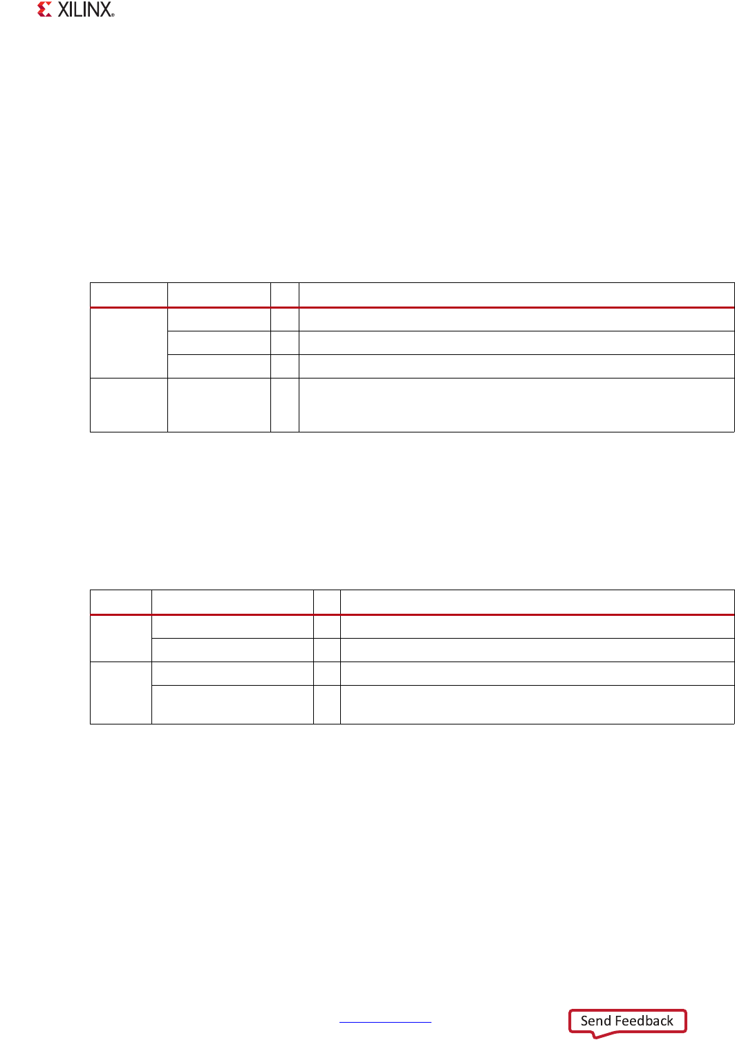
Table 2-9: PL Interrupt Signals
Type PL Signal Name I/O Destination
PL to PS
Interrupts
IRQF2P[7:0] I SPI: Numbers [68:61].
IRQF2P[15:8] I SPI: Numbers [91:84].
IRQF2P[19:16] I PPI: nFIQ, nIRQ (both CPUs).
PS to PL
Interrupts
IRQP2F[27:0] O
Pl Logic. These signals are received from the I/O peripherals and are
forwarded to the interrupt controller. These signals are also provided as
outputs to the PL.
Table 2-10: PL Event Signals
Type PL Signal Name I/O Description
Events
EVENTEVENTI I Causes one or both CPUs to wake up from a WFE state.
EVENTEVENTO O Asserted when one of the CPUs has executed the SEV instruction.
Standby
EVENTSTANDBYWFE[1:0] O CPU standby mode: asserted when a CPU is waiting for an event.
EVENTSTANDBYWFI[1:0] O
CPU standby mode: asserted when a CPU is waiting for an
interrupt.