
User manual


Table Of Contents
- Zynq-7000 All Programmable SoC
- Table of Contents
- Ch. 1: Introduction
- Ch. 2: Signals, Interfaces, and Pins
- Ch. 3: Application Processing Unit
- Ch. 4: System Addresses
- Ch. 5: Interconnect
- Ch. 6: Boot and Configuration
- Ch. 7: Interrupts
- Ch. 8: Timers
- Ch. 9: DMA Controller
- Introduction
- Functional Description
- DMA Transfers on the AXI Interconnect
- AXI Transaction Considerations
- DMA Manager
- Multi-channel Data FIFO (MFIFO)
- Memory-to-Memory Transfers
- PL Peripheral AXI Transactions
- PL Peripheral Request Interface
- PL Peripheral - Length Managed by PL Peripheral
- PL Peripheral - Length Managed by DMAC
- Events and Interrupts
- Aborts
- Security
- IP Configuration Options
- Programming Guide for DMA Controller
- Programming Guide for DMA Engine
- Programming Restrictions
- System Functions
- I/O Interface
- Ch. 10: DDR Memory Controller
- Introduction
- AXI Memory Port Interface (DDRI)
- DDR Core and Transaction Scheduler (DDRC)
- DDRC Arbitration
- Controller PHY (DDRP)
- Initialization and Calibration
- DDR Clock Initialization
- DDR IOB Impedance Calibration
- DDR IOB Configuration
- DDR Controller Register Programming
- DRAM Reset and Initialization
- DRAM Input Impedance (ODT) Calibration
- DRAM Output Impedance (RON) Calibration
- DRAM Training
- Write Data Eye Adjustment
- Alternatives to Automatic DRAM Training
- DRAM Write Latency Restriction
- Register Overview
- Error Correction Code (ECC)
- Programming Model
- Ch. 11: Static Memory Controller
- Ch. 12: Quad-SPI Flash Controller
- Ch. 13: SD/SDIO Controller
- Ch. 14: General Purpose I/O (GPIO)
- Ch. 15: USB Host, Device, and OTG Controller
- Introduction
- Functional Description
- Programming Overview and Reference
- Device Mode Control
- Device Endpoint Data Structures
- Device Endpoint Packet Operational Model
- Device Endpoint Descriptor Reference
- Programming Guide for Device Controller
- Programming Guide for Device Endpoint Data Structures
- Host Mode Data Structures
- EHCI Implementation
- Host Data Structures Reference
- Programming Guide for Host Controller
- OTG Description and Reference
- System Functions
- I/O Interfaces
- Ch. 16: Gigabit Ethernet Controller
- Ch. 17: SPI Controller
- Ch. 18: CAN Controller
- Ch. 19: UART Controller
- Ch. 20: I2C Controller
- Ch. 21: Programmable Logic Description
- Ch. 22: Programmable Logic Design Guide
- Ch. 23: Programmable Logic Test and Debug
- Ch. 24: Power Management
- Ch. 25: Clocks
- Ch. 26: Reset System
- Ch. 27: JTAG and DAP Subsystem
- Ch. 28: System Test and Debug
- Ch. 29: On-Chip Memory (OCM)
- Ch. 30: XADC Interface
- Ch. 31: PCI Express
- Ch. 32: Device Secure Boot
- Appx. A: Additional Resources
- Appx. B: Register Details
- Overview
- Acronyms
- Module Summary
- AXI_HP Interface (AFI) (axi_hp)
- CAN Controller (can)
- DDR Memory Controller (ddrc)
- CoreSight Cross Trigger Interface (cti)
- Performance Monitor Unit (cortexa9_pmu)
- CoreSight Program Trace Macrocell (ptm)
- Debug Access Port (dap)
- CoreSight Embedded Trace Buffer (etb)
- PL Fabric Trace Monitor (ftm)
- CoreSight Trace Funnel (funnel)
- CoreSight Intstrumentation Trace Macrocell (itm)
- CoreSight Trace Packet Output (tpiu)
- Device Configuration Interface (devcfg)
- DMA Controller (dmac)
- Gigabit Ethernet Controller (GEM)
- General Purpose I/O (gpio)
- Interconnect QoS (qos301)
- NIC301 Address Region Control (nic301_addr_region_ctrl_registers)
- I2C Controller (IIC)
- L2 Cache (L2Cpl310)
- Application Processing Unit (mpcore)
- On-Chip Memory (ocm)
- Quad-SPI Flash Controller (qspi)
- SD Controller (sdio)
- System Level Control Registers (slcr)
- Static Memory Controller (pl353)
- SPI Controller (SPI)
- System Watchdog Timer (swdt)
- Triple Timer Counter (ttc)
- UART Controller (UART)
- USB Controller (usb)
Zynq-7000 AP SoC Technical Reference Manual www.xilinx.com 584
UG585 (v1.11) September 27, 2016
Chapter 19: UART Controller
• Loop UART 0 with UART 1 option
• Modem control signals: CTS, RTS, DSR, DTR, RI and DCD are available only on the EMIO interface
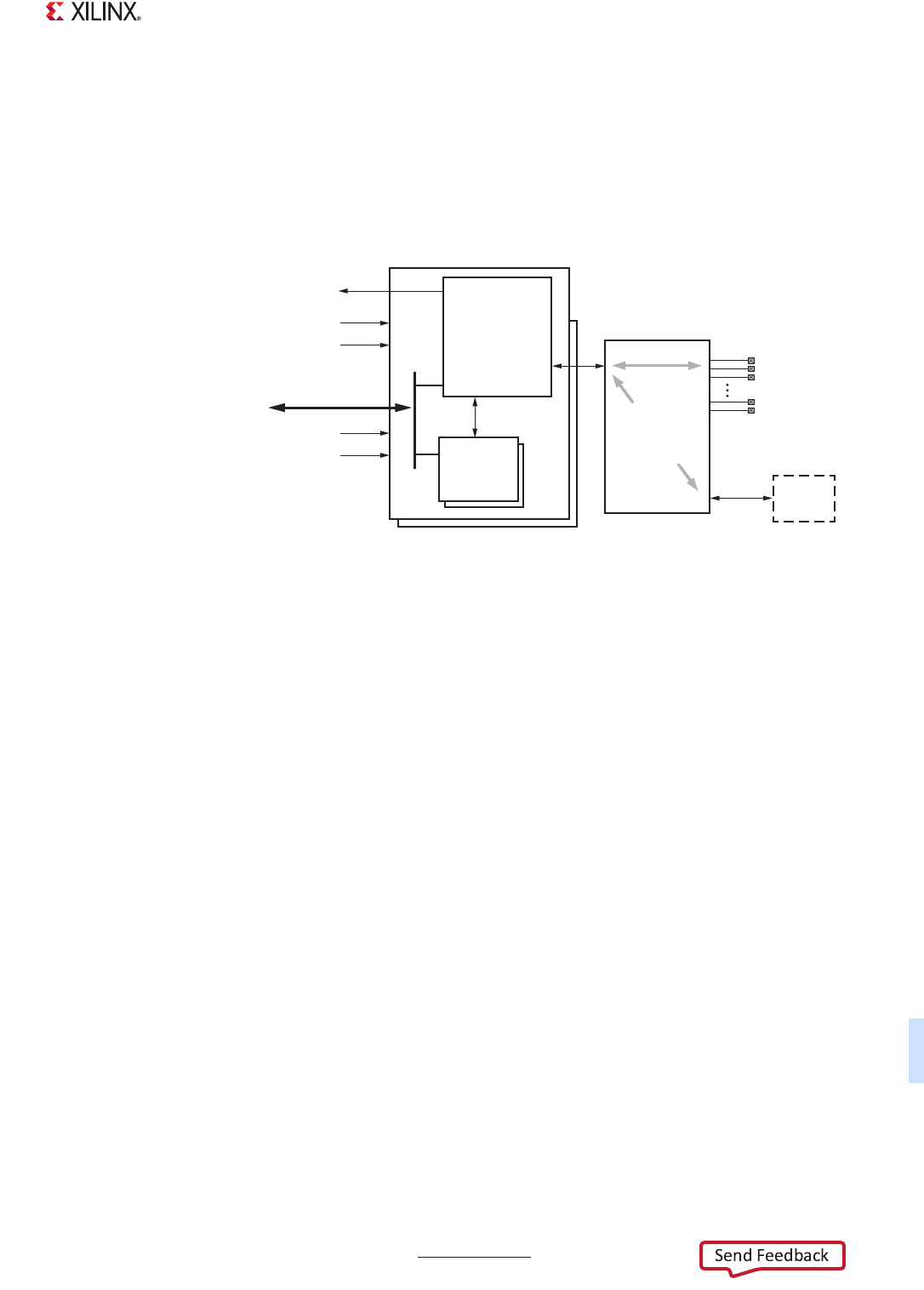
19.1.2 System Viewpoint
The system viewpoint diagram for the UART controllers is shown in Figure 19-1.
The slcr register set (refer to section 4.3 SLCR Registers) includes control bits for the UART clocks,
resets and MIO-EMIO signal mapping. Software accesses the UART controller registers using the APB
32-bit slave interface attached to the PS AXI interconnect. The IRQ from each controller is connected
to the PS interrupt controller and routed to the PL.
19.1.3 Notices
Reference Clock Operating Restrictions
There is a single PS clock generator for both UART controllers. The reference clocks (UART_Ref_Clk)
going to the baud rate generator of each UART controller are of the same clock frequency, but are
individually enabled, refer to section 25.6.3 SDIO, SMC, SPI, Quad-SPI and UART Clocks. The
controllers are always clocked by the internal, PS clock generator.
Note: There are no frequency restrictions in the relationship between the CPU_1x and UART_Ref_clk
clocks.
7z007s and 7z010 CLG225 Devices
The 7z007s single core and 7z010 dual core CLG225 devices support 32 MIO pins as shown in the
MIO-at-a-Glance Table, page 52. This restricts the availability of the UART signals on the MIO pins. If
needed, the TxD and RxD UART signals can be routed through the EMIO interface and
passed-through to the PL pins. All of the CLG225 device restrictions are listed in section
1.1.3 Notices.
X-Ref Target - Figure 19-1
Figure 19-1: UART System Viewpoint
PL
MIO – EMIO
Routing
PS Slave
Interconnect
APB
MIO
Pins
UG585_c19_01_010112
EMIO
Signals
UART REF_CLK
IRQ ID# {59, 82}
UART REF_RST
Control
And Status
Registers
Slave
ports
Tx, Rx
Tx, Rx, CTSN,
DCDN, DSRN,
RIN, DTRN,
RTSN
CPU_1x clock
UART{0, 1} CPU1X_RST
UART
Interface
Controller