
User manual


Table Of Contents
- Zynq-7000 All Programmable SoC
- Table of Contents
- Ch. 1: Introduction
- Ch. 2: Signals, Interfaces, and Pins
- Ch. 3: Application Processing Unit
- Ch. 4: System Addresses
- Ch. 5: Interconnect
- Ch. 6: Boot and Configuration
- Ch. 7: Interrupts
- Ch. 8: Timers
- Ch. 9: DMA Controller
- Introduction
- Functional Description
- DMA Transfers on the AXI Interconnect
- AXI Transaction Considerations
- DMA Manager
- Multi-channel Data FIFO (MFIFO)
- Memory-to-Memory Transfers
- PL Peripheral AXI Transactions
- PL Peripheral Request Interface
- PL Peripheral - Length Managed by PL Peripheral
- PL Peripheral - Length Managed by DMAC
- Events and Interrupts
- Aborts
- Security
- IP Configuration Options
- Programming Guide for DMA Controller
- Programming Guide for DMA Engine
- Programming Restrictions
- System Functions
- I/O Interface
- Ch. 10: DDR Memory Controller
- Introduction
- AXI Memory Port Interface (DDRI)
- DDR Core and Transaction Scheduler (DDRC)
- DDRC Arbitration
- Controller PHY (DDRP)
- Initialization and Calibration
- DDR Clock Initialization
- DDR IOB Impedance Calibration
- DDR IOB Configuration
- DDR Controller Register Programming
- DRAM Reset and Initialization
- DRAM Input Impedance (ODT) Calibration
- DRAM Output Impedance (RON) Calibration
- DRAM Training
- Write Data Eye Adjustment
- Alternatives to Automatic DRAM Training
- DRAM Write Latency Restriction
- Register Overview
- Error Correction Code (ECC)
- Programming Model
- Ch. 11: Static Memory Controller
- Ch. 12: Quad-SPI Flash Controller
- Ch. 13: SD/SDIO Controller
- Ch. 14: General Purpose I/O (GPIO)
- Ch. 15: USB Host, Device, and OTG Controller
- Introduction
- Functional Description
- Programming Overview and Reference
- Device Mode Control
- Device Endpoint Data Structures
- Device Endpoint Packet Operational Model
- Device Endpoint Descriptor Reference
- Programming Guide for Device Controller
- Programming Guide for Device Endpoint Data Structures
- Host Mode Data Structures
- EHCI Implementation
- Host Data Structures Reference
- Programming Guide for Host Controller
- OTG Description and Reference
- System Functions
- I/O Interfaces
- Ch. 16: Gigabit Ethernet Controller
- Ch. 17: SPI Controller
- Ch. 18: CAN Controller
- Ch. 19: UART Controller
- Ch. 20: I2C Controller
- Ch. 21: Programmable Logic Description
- Ch. 22: Programmable Logic Design Guide
- Ch. 23: Programmable Logic Test and Debug
- Ch. 24: Power Management
- Ch. 25: Clocks
- Ch. 26: Reset System
- Ch. 27: JTAG and DAP Subsystem
- Ch. 28: System Test and Debug
- Ch. 29: On-Chip Memory (OCM)
- Ch. 30: XADC Interface
- Ch. 31: PCI Express
- Ch. 32: Device Secure Boot
- Appx. A: Additional Resources
- Appx. B: Register Details
- Overview
- Acronyms
- Module Summary
- AXI_HP Interface (AFI) (axi_hp)
- CAN Controller (can)
- DDR Memory Controller (ddrc)
- CoreSight Cross Trigger Interface (cti)
- Performance Monitor Unit (cortexa9_pmu)
- CoreSight Program Trace Macrocell (ptm)
- Debug Access Port (dap)
- CoreSight Embedded Trace Buffer (etb)
- PL Fabric Trace Monitor (ftm)
- CoreSight Trace Funnel (funnel)
- CoreSight Intstrumentation Trace Macrocell (itm)
- CoreSight Trace Packet Output (tpiu)
- Device Configuration Interface (devcfg)
- DMA Controller (dmac)
- Gigabit Ethernet Controller (GEM)
- General Purpose I/O (gpio)
- Interconnect QoS (qos301)
- NIC301 Address Region Control (nic301_addr_region_ctrl_registers)
- I2C Controller (IIC)
- L2 Cache (L2Cpl310)
- Application Processing Unit (mpcore)
- On-Chip Memory (ocm)
- Quad-SPI Flash Controller (qspi)
- SD Controller (sdio)
- System Level Control Registers (slcr)
- Static Memory Controller (pl353)
- SPI Controller (SPI)
- System Watchdog Timer (swdt)
- Triple Timer Counter (ttc)
- UART Controller (UART)
- USB Controller (usb)
Zynq-7000 AP SoC Technical Reference Manual www.xilinx.com 587
UG585 (v1.11) September 27, 2016
Chapter 19: UART Controller
values for CD and BDIV. For these examples, a system clock rate of UART_Ref_Clk = 50 MHz and
Uart_ref_clk/8 = 6.25 MHz is assumed. The frequency of the UART reference clock can be changed to
get a more accurate Baud rate frequency, refer to Chapter 25, Clocks for details to program the
UART_Ref_Clk.
19.2.4 Transmit FIFO
The transmit FIFO (TxFIFO) stores data written from the APB interface until it is removed by the
transmit module and loaded into its shift register. The TxFIFO’s maximum data width is eight bits.
Data is loaded into the TxFIFO by writing to the TxFIFO register.
When data is loaded into the TxFIFO, the TxFIFO empty flag is cleared and remains in this Low state
until the last word in the TxFIFO has been removed and loaded into the transmitter shift register. This
means that host software has another full serial word time until the next data is needed, allowing it
to react to the empty flag being set and write another word in the TxFIFO without loss in transmission
time.
The TxFIFO full interrupt status (TFULL) indicates that the TxFIFO is completely full and prevents any
further data from being loaded into the TxFIFO. If another APB write to the TxFIFO is performed, an
overflow is triggered and the write data is not loaded into the TxFIFO. The transmit FIFO nearly full
flag (TNFULL) indicates that there is not enough free space in the FIFO for one more write of the
programmed size, as controlled by the WSIZE bits of the Mode register.
The TxFIFO nearly-full flag (TNFULL) indicates that there is only byte free in the TxFIFO.
A threshold trigger (TTRIG) can be setup on the TxFIFO fill level. The Transmitter Trigger register can
be used to setup this value, such that the trigger is set when the TxFIFO fill level reaches this
programmed value.
19.2.5 Transmitter Data Stream
The transmit module removes parallel data from the TxFIFO and loads it into the transmitter shift
register so that it can be serialized.
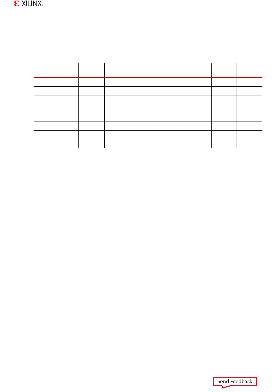
Table 19-1: UART Parameter Value Examples
Clock
Baud
Rate
Calculated
CD
Actual
CD
BDIV
Actual
Baud Rate
Error
(BPS)
% Error
UART Ref clock 600 10416.667 10417 7 599.980 0.020 -0.003
UART Ref clock /8 9,600 81.380 81 7 9,645.061 45.061 0.469
UART Ref clock 9,600 651.041 651 7 9,600.614 0.614 0.006
UART Ref clock 28,800 347.222 347 4 28,818.44 18.44 0.064
UART Ref clock 115,200 62.004 62 6 115,207.37 7.373 0.0064
UART Ref clock 230,400 31.002 31 6 230,414.75 14.75 0.006
UART Ref clock 460,800 27.127 9 11 462,962.96 2,162.96 0.469
UART Ref clock 921,600 9.042 9 5 925,925.92 4,325.93 0.469