
User manual


Table Of Contents
- Zynq-7000 All Programmable SoC
- Table of Contents
- Ch. 1: Introduction
- Ch. 2: Signals, Interfaces, and Pins
- Ch. 3: Application Processing Unit
- Ch. 4: System Addresses
- Ch. 5: Interconnect
- Ch. 6: Boot and Configuration
- Ch. 7: Interrupts
- Ch. 8: Timers
- Ch. 9: DMA Controller
- Introduction
- Functional Description
- DMA Transfers on the AXI Interconnect
- AXI Transaction Considerations
- DMA Manager
- Multi-channel Data FIFO (MFIFO)
- Memory-to-Memory Transfers
- PL Peripheral AXI Transactions
- PL Peripheral Request Interface
- PL Peripheral - Length Managed by PL Peripheral
- PL Peripheral - Length Managed by DMAC
- Events and Interrupts
- Aborts
- Security
- IP Configuration Options
- Programming Guide for DMA Controller
- Programming Guide for DMA Engine
- Programming Restrictions
- System Functions
- I/O Interface
- Ch. 10: DDR Memory Controller
- Introduction
- AXI Memory Port Interface (DDRI)
- DDR Core and Transaction Scheduler (DDRC)
- DDRC Arbitration
- Controller PHY (DDRP)
- Initialization and Calibration
- DDR Clock Initialization
- DDR IOB Impedance Calibration
- DDR IOB Configuration
- DDR Controller Register Programming
- DRAM Reset and Initialization
- DRAM Input Impedance (ODT) Calibration
- DRAM Output Impedance (RON) Calibration
- DRAM Training
- Write Data Eye Adjustment
- Alternatives to Automatic DRAM Training
- DRAM Write Latency Restriction
- Register Overview
- Error Correction Code (ECC)
- Programming Model
- Ch. 11: Static Memory Controller
- Ch. 12: Quad-SPI Flash Controller
- Ch. 13: SD/SDIO Controller
- Ch. 14: General Purpose I/O (GPIO)
- Ch. 15: USB Host, Device, and OTG Controller
- Introduction
- Functional Description
- Programming Overview and Reference
- Device Mode Control
- Device Endpoint Data Structures
- Device Endpoint Packet Operational Model
- Device Endpoint Descriptor Reference
- Programming Guide for Device Controller
- Programming Guide for Device Endpoint Data Structures
- Host Mode Data Structures
- EHCI Implementation
- Host Data Structures Reference
- Programming Guide for Host Controller
- OTG Description and Reference
- System Functions
- I/O Interfaces
- Ch. 16: Gigabit Ethernet Controller
- Ch. 17: SPI Controller
- Ch. 18: CAN Controller
- Ch. 19: UART Controller
- Ch. 20: I2C Controller
- Ch. 21: Programmable Logic Description
- Ch. 22: Programmable Logic Design Guide
- Ch. 23: Programmable Logic Test and Debug
- Ch. 24: Power Management
- Ch. 25: Clocks
- Ch. 26: Reset System
- Ch. 27: JTAG and DAP Subsystem
- Ch. 28: System Test and Debug
- Ch. 29: On-Chip Memory (OCM)
- Ch. 30: XADC Interface
- Ch. 31: PCI Express
- Ch. 32: Device Secure Boot
- Appx. A: Additional Resources
- Appx. B: Register Details
- Overview
- Acronyms
- Module Summary
- AXI_HP Interface (AFI) (axi_hp)
- CAN Controller (can)
- DDR Memory Controller (ddrc)
- CoreSight Cross Trigger Interface (cti)
- Performance Monitor Unit (cortexa9_pmu)
- CoreSight Program Trace Macrocell (ptm)
- Debug Access Port (dap)
- CoreSight Embedded Trace Buffer (etb)
- PL Fabric Trace Monitor (ftm)
- CoreSight Trace Funnel (funnel)
- CoreSight Intstrumentation Trace Macrocell (itm)
- CoreSight Trace Packet Output (tpiu)
- Device Configuration Interface (devcfg)
- DMA Controller (dmac)
- Gigabit Ethernet Controller (GEM)
- General Purpose I/O (gpio)
- Interconnect QoS (qos301)
- NIC301 Address Region Control (nic301_addr_region_ctrl_registers)
- I2C Controller (IIC)
- L2 Cache (L2Cpl310)
- Application Processing Unit (mpcore)
- On-Chip Memory (ocm)
- Quad-SPI Flash Controller (qspi)
- SD Controller (sdio)
- System Level Control Registers (slcr)
- Static Memory Controller (pl353)
- SPI Controller (SPI)
- System Watchdog Timer (swdt)
- Triple Timer Counter (ttc)
- UART Controller (UART)
- USB Controller (usb)
Zynq-7000 AP SoC Technical Reference Manual www.xilinx.com 589
UG585 (v1.11) September 27, 2016
Chapter 19: UART Controller
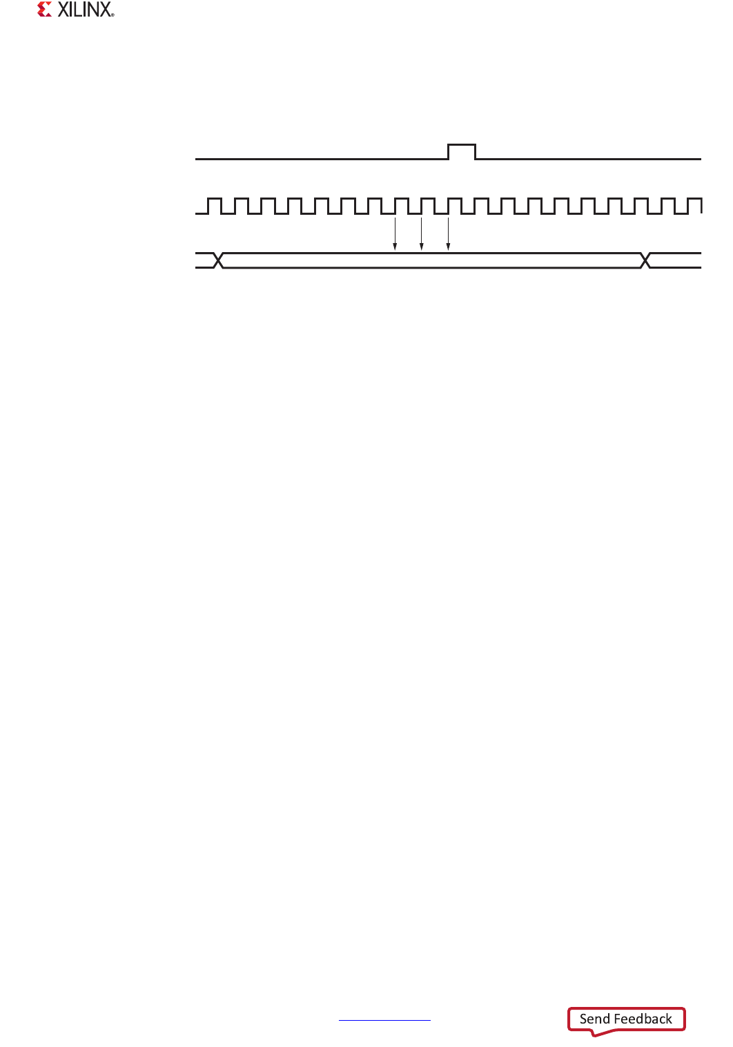
When a valid start bit is identified, the receiver baud rate clock enable (baud_rx_rate) is
re-synchronised so that further sampling of the incoming UART RxD signal occurs around the
theoretical mid-point of each bit, as illustrated in Figure 19-6.
When the re-synchronised baud_rx_rate is High, the last three sampled bits are compared. The logic
value is determined by majority voting; two samples having the same value define the value of the
data bit. When the value of a serial data bit has been determined, it is shifted to the receive shift
register. When a complete character has been assembled, the contents of the register are then
pushed to the RxFIFO.
Receiver Parity Error
Each time a character is received, the receiver calculates the parity of the received data bits in
accordance with the uart.mode_reg0 [PAR] bit field. It then compares the result with the received
parity bit. If a difference is detected, the parity error bit is set = 1, uart.Chnl_int_sts_reg0 [PARE]. An
interrupt is generated, if enabled.
Receiver Framing Error
When the receiver fails to receive a valid stop bit at the end of a frame, the frame error bit is set =1,
uart.Chnl_int_sts_reg0 [FRAME]. An interrupt is generated, if enabled.
Receiver Overflow Error
When a character is received, the controller checks to see if the RxFIFO has room. If it does, then the
character is written into the RxFIFO. If the RxFIFO is full, then the controller waits. If a subsequent
start bit on RxD is detected and the RxFIFO is still full, then data is lost and the controller sets the Rx
overflow interrupt bit, uart.Chnl_int_sts_reg0 [ROVR] = 1. An interrupt is generated, if enabled.
Receiver Timeout Mechanism
The receiver timeout mechanism enables the receiver to detect an inactive RxD signal (a persistent
High level). The timeout period is programmed by writing to the uart.Rcvr_timeout_reg0 [RTO] bit
field. The timeout mechanism uses a 10-bit decrementing counter. The counter is reloaded and starts
counting down whenever a new start bit is received on the RxD signal, or whenever software writes
a 1 to uart.Control_reg0 [RSTTO] (regardless of the previous [RSTTO] value).
X-Ref Target - Figure 19-6
Figure 19-6: Re-synchronized Receiver Data Stream
baud_sample
baud_rx_rate
rxd
12345678
Data Bit
9 10111213141516 1 2
UG585_c19_06_022612