
User manual


Table Of Contents
- Zynq-7000 All Programmable SoC
- Table of Contents
- Ch. 1: Introduction
- Ch. 2: Signals, Interfaces, and Pins
- Ch. 3: Application Processing Unit
- Ch. 4: System Addresses
- Ch. 5: Interconnect
- Ch. 6: Boot and Configuration
- Ch. 7: Interrupts
- Ch. 8: Timers
- Ch. 9: DMA Controller
- Introduction
- Functional Description
- DMA Transfers on the AXI Interconnect
- AXI Transaction Considerations
- DMA Manager
- Multi-channel Data FIFO (MFIFO)
- Memory-to-Memory Transfers
- PL Peripheral AXI Transactions
- PL Peripheral Request Interface
- PL Peripheral - Length Managed by PL Peripheral
- PL Peripheral - Length Managed by DMAC
- Events and Interrupts
- Aborts
- Security
- IP Configuration Options
- Programming Guide for DMA Controller
- Programming Guide for DMA Engine
- Programming Restrictions
- System Functions
- I/O Interface
- Ch. 10: DDR Memory Controller
- Introduction
- AXI Memory Port Interface (DDRI)
- DDR Core and Transaction Scheduler (DDRC)
- DDRC Arbitration
- Controller PHY (DDRP)
- Initialization and Calibration
- DDR Clock Initialization
- DDR IOB Impedance Calibration
- DDR IOB Configuration
- DDR Controller Register Programming
- DRAM Reset and Initialization
- DRAM Input Impedance (ODT) Calibration
- DRAM Output Impedance (RON) Calibration
- DRAM Training
- Write Data Eye Adjustment
- Alternatives to Automatic DRAM Training
- DRAM Write Latency Restriction
- Register Overview
- Error Correction Code (ECC)
- Programming Model
- Ch. 11: Static Memory Controller
- Ch. 12: Quad-SPI Flash Controller
- Ch. 13: SD/SDIO Controller
- Ch. 14: General Purpose I/O (GPIO)
- Ch. 15: USB Host, Device, and OTG Controller
- Introduction
- Functional Description
- Programming Overview and Reference
- Device Mode Control
- Device Endpoint Data Structures
- Device Endpoint Packet Operational Model
- Device Endpoint Descriptor Reference
- Programming Guide for Device Controller
- Programming Guide for Device Endpoint Data Structures
- Host Mode Data Structures
- EHCI Implementation
- Host Data Structures Reference
- Programming Guide for Host Controller
- OTG Description and Reference
- System Functions
- I/O Interfaces
- Ch. 16: Gigabit Ethernet Controller
- Ch. 17: SPI Controller
- Ch. 18: CAN Controller
- Ch. 19: UART Controller
- Ch. 20: I2C Controller
- Ch. 21: Programmable Logic Description
- Ch. 22: Programmable Logic Design Guide
- Ch. 23: Programmable Logic Test and Debug
- Ch. 24: Power Management
- Ch. 25: Clocks
- Ch. 26: Reset System
- Ch. 27: JTAG and DAP Subsystem
- Ch. 28: System Test and Debug
- Ch. 29: On-Chip Memory (OCM)
- Ch. 30: XADC Interface
- Ch. 31: PCI Express
- Ch. 32: Device Secure Boot
- Appx. A: Additional Resources
- Appx. B: Register Details
- Overview
- Acronyms
- Module Summary
- AXI_HP Interface (AFI) (axi_hp)
- CAN Controller (can)
- DDR Memory Controller (ddrc)
- CoreSight Cross Trigger Interface (cti)
- Performance Monitor Unit (cortexa9_pmu)
- CoreSight Program Trace Macrocell (ptm)
- Debug Access Port (dap)
- CoreSight Embedded Trace Buffer (etb)
- PL Fabric Trace Monitor (ftm)
- CoreSight Trace Funnel (funnel)
- CoreSight Intstrumentation Trace Macrocell (itm)
- CoreSight Trace Packet Output (tpiu)
- Device Configuration Interface (devcfg)
- DMA Controller (dmac)
- Gigabit Ethernet Controller (GEM)
- General Purpose I/O (gpio)
- Interconnect QoS (qos301)
- NIC301 Address Region Control (nic301_addr_region_ctrl_registers)
- I2C Controller (IIC)
- L2 Cache (L2Cpl310)
- Application Processing Unit (mpcore)
- On-Chip Memory (ocm)
- Quad-SPI Flash Controller (qspi)
- SD Controller (sdio)
- System Level Control Registers (slcr)
- Static Memory Controller (pl353)
- SPI Controller (SPI)
- System Watchdog Timer (swdt)
- Triple Timer Counter (ttc)
- UART Controller (UART)
- USB Controller (usb)
Zynq-7000 AP SoC Technical Reference Manual www.xilinx.com 622
UG585 (v1.11) September 27, 2016
Chapter 21: Programmable Logic Description
21.1.3 Notices
XADC Analog Mixed Signal Module (AMS)
The XADC is physically located in the PL and is powered by the PL. To use the XADC module, the PL
must be powered up, but the PL does not need to be configured. The XADC is explained in
Chapter 30, XADC Interface.
Device Configuration (DevC)
The device configuration module (with option to use AES/HMAC decryption) is physically located in
the PL and is powered by the PL. To use the device configuration module, the PL must be powered
up but does not need to be configured. Device configuration is explained in section 6.4 Device Boot
and PL Configuration.
21.2 PL Components
21.2.1 CLBs, Slices, and LUTs
A CLB element contains a pair of slices, and each slice is composed of four 6-input Look Up Tables (LUTs)
and eight storage elements.
• SLICE(0) - slice at the bottom of the CLB and in the left column.
• SLICE(1) - slice at the top of the CLB and in the right column.
These two slices do not have direct connections to each other, and each slice is organized as a column. Each
slice in a column has an independent carry chain. The LUTs have the following features:
• Single 6 input LUT with one output, or two 5 input LUTs.
• Memory capability within the LUT.
• Register and shift register functionality.
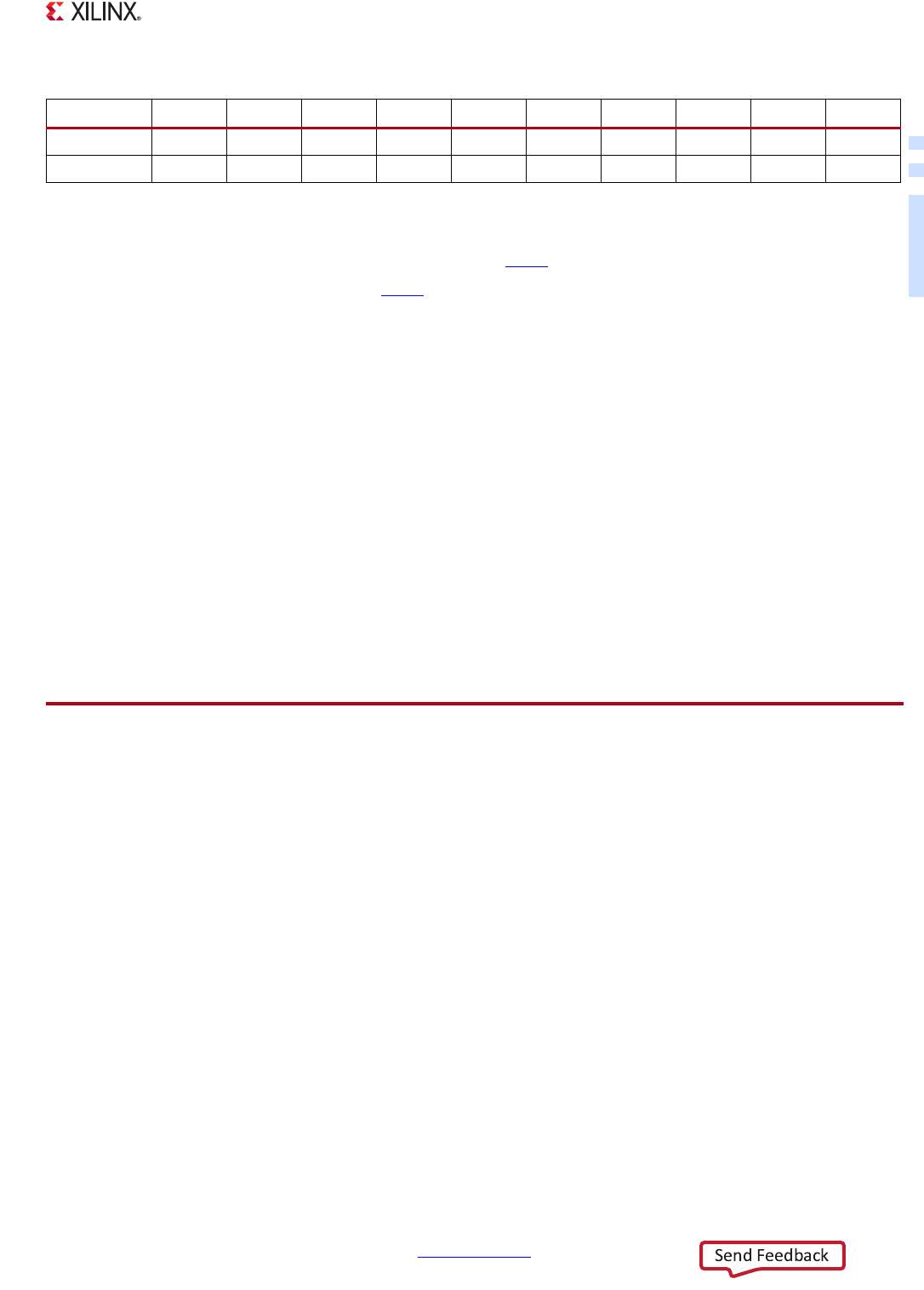
HR 100 150 200 100 150 200 100 250 250 250
HP 100 150 200 000 150 200 100 250 250 250
Notes:
1. Number of slices corresponding to the number of flip-flops and LUTRAM supported in the device.
2. The total count is limited by tools.
3. The number of transceivers in the 7z035 and 7z045 devices depends on the package type. Refer to the Serial Transceiver Channels
by Device/Package table in the Zynq-7000 AP SoC Packaging Guide (UG865
) for exact counts.
4. This table shows the maximum I/Os that are available for each device type. The package size might restrict the SelectIO pin counts,
refer to the Zynq-7000 AP SoC Packaging Guide (UG865
).
Table 21-1: PL Resources by Device Type (Cont’d)
Resource 7z007s 7z012s 7z014s 7z010 7z015 7z020 7z030 7z035 7z045 7z100