
User manual


Table Of Contents
- Zynq-7000 All Programmable SoC
- Table of Contents
- Ch. 1: Introduction
- Ch. 2: Signals, Interfaces, and Pins
- Ch. 3: Application Processing Unit
- Ch. 4: System Addresses
- Ch. 5: Interconnect
- Ch. 6: Boot and Configuration
- Ch. 7: Interrupts
- Ch. 8: Timers
- Ch. 9: DMA Controller
- Introduction
- Functional Description
- DMA Transfers on the AXI Interconnect
- AXI Transaction Considerations
- DMA Manager
- Multi-channel Data FIFO (MFIFO)
- Memory-to-Memory Transfers
- PL Peripheral AXI Transactions
- PL Peripheral Request Interface
- PL Peripheral - Length Managed by PL Peripheral
- PL Peripheral - Length Managed by DMAC
- Events and Interrupts
- Aborts
- Security
- IP Configuration Options
- Programming Guide for DMA Controller
- Programming Guide for DMA Engine
- Programming Restrictions
- System Functions
- I/O Interface
- Ch. 10: DDR Memory Controller
- Introduction
- AXI Memory Port Interface (DDRI)
- DDR Core and Transaction Scheduler (DDRC)
- DDRC Arbitration
- Controller PHY (DDRP)
- Initialization and Calibration
- DDR Clock Initialization
- DDR IOB Impedance Calibration
- DDR IOB Configuration
- DDR Controller Register Programming
- DRAM Reset and Initialization
- DRAM Input Impedance (ODT) Calibration
- DRAM Output Impedance (RON) Calibration
- DRAM Training
- Write Data Eye Adjustment
- Alternatives to Automatic DRAM Training
- DRAM Write Latency Restriction
- Register Overview
- Error Correction Code (ECC)
- Programming Model
- Ch. 11: Static Memory Controller
- Ch. 12: Quad-SPI Flash Controller
- Ch. 13: SD/SDIO Controller
- Ch. 14: General Purpose I/O (GPIO)
- Ch. 15: USB Host, Device, and OTG Controller
- Introduction
- Functional Description
- Programming Overview and Reference
- Device Mode Control
- Device Endpoint Data Structures
- Device Endpoint Packet Operational Model
- Device Endpoint Descriptor Reference
- Programming Guide for Device Controller
- Programming Guide for Device Endpoint Data Structures
- Host Mode Data Structures
- EHCI Implementation
- Host Data Structures Reference
- Programming Guide for Host Controller
- OTG Description and Reference
- System Functions
- I/O Interfaces
- Ch. 16: Gigabit Ethernet Controller
- Ch. 17: SPI Controller
- Ch. 18: CAN Controller
- Ch. 19: UART Controller
- Ch. 20: I2C Controller
- Ch. 21: Programmable Logic Description
- Ch. 22: Programmable Logic Design Guide
- Ch. 23: Programmable Logic Test and Debug
- Ch. 24: Power Management
- Ch. 25: Clocks
- Ch. 26: Reset System
- Ch. 27: JTAG and DAP Subsystem
- Ch. 28: System Test and Debug
- Ch. 29: On-Chip Memory (OCM)
- Ch. 30: XADC Interface
- Ch. 31: PCI Express
- Ch. 32: Device Secure Boot
- Appx. A: Additional Resources
- Appx. B: Register Details
- Overview
- Acronyms
- Module Summary
- AXI_HP Interface (AFI) (axi_hp)
- CAN Controller (can)
- DDR Memory Controller (ddrc)
- CoreSight Cross Trigger Interface (cti)
- Performance Monitor Unit (cortexa9_pmu)
- CoreSight Program Trace Macrocell (ptm)
- Debug Access Port (dap)
- CoreSight Embedded Trace Buffer (etb)
- PL Fabric Trace Monitor (ftm)
- CoreSight Trace Funnel (funnel)
- CoreSight Intstrumentation Trace Macrocell (itm)
- CoreSight Trace Packet Output (tpiu)
- Device Configuration Interface (devcfg)
- DMA Controller (dmac)
- Gigabit Ethernet Controller (GEM)
- General Purpose I/O (gpio)
- Interconnect QoS (qos301)
- NIC301 Address Region Control (nic301_addr_region_ctrl_registers)
- I2C Controller (IIC)
- L2 Cache (L2Cpl310)
- Application Processing Unit (mpcore)
- On-Chip Memory (ocm)
- Quad-SPI Flash Controller (qspi)
- SD Controller (sdio)
- System Level Control Registers (slcr)
- Static Memory Controller (pl353)
- SPI Controller (SPI)
- System Watchdog Timer (swdt)
- Triple Timer Counter (ttc)
- UART Controller (UART)
- USB Controller (usb)
Zynq-7000 AP SoC Technical Reference Manual www.xilinx.com 652
UG585 (v1.11) September 27, 2016
Chapter 22: Programmable Logic Design Guide
22.3 PL and Memory System Performance Overview
This section provides a comparison of various performance-related behaviors of memory paths
through the PS. It is intended to familiarize the designer with the performance-related behaviors of
the PL and PS memory system.
22.3.1 Theoretical Bandwidth
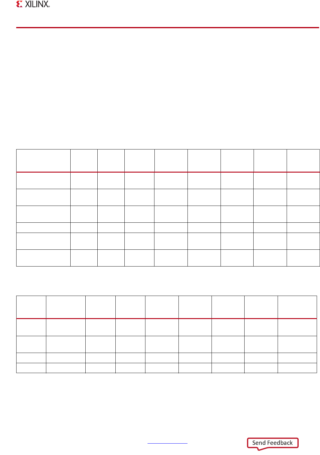
Table 22-2 and Table 22-3 provide a basic introduction of relative performance capabilities between
various programmable interfaces, DMA, and memory controllers. The bandwidth are calculated as
the interface width multiplied by a typical clock rate, not including any protocol overhead.
Table 22-2: Theoretical Bandwidth of PS-PL and PS Memory Interfaces
Interface Type
Bus
Width
(bits)
IF Clock
(MHz)
Read
Bandwidth
(MB/s)
Write
Bandwidth
(MB/s)
R+W
Bandwidth
(MB/s)
Number of
Interfaces
Total
Bandwidth
(MB/s)
General Purpose
AXI
PS Slave 32 150 600 600 1,200 2 2,400
General Purpose
AXI
PS
Master
32 150 600 600 1,200 2 2,400
High Performance
(AFI) AXI_HP
PS Slave 64 150 1,200 1,200 2,400 4 9,600
AXI _ACP PS Slave 64 150 1,200 1,200 2,400 1 2,400
DDR
External
Memory
32 1,066 4,264 4,264 4,264 1 4,264
OCM
Internal
Memory
64 222 1,779 1,779 3,557 1 3,557
Table 22-3: Theoretical Bandwidth of PS DMA Controllers
DMA Type
IF Width
(Bits)
IF Clock
(MHz)
Read BW
(MB/s)
Write BW
(MB/s)
R+W BW
(MB/s)
Number of
Interfaces
Total
Bandwidth
(MB/s)
DMAC ARM PL310 64 222 1,776 1,776 3,552 1 3,552
Gigabit
Ethernet
PS Master 4 250 125 125 250 2 500
USB PS Master 8 60 60 60 60 2 120
SD PS Master 4 50 25 25 25 2 50