
User manual


Table Of Contents
- Zynq-7000 All Programmable SoC
- Table of Contents
- Ch. 1: Introduction
- Ch. 2: Signals, Interfaces, and Pins
- Ch. 3: Application Processing Unit
- Ch. 4: System Addresses
- Ch. 5: Interconnect
- Ch. 6: Boot and Configuration
- Ch. 7: Interrupts
- Ch. 8: Timers
- Ch. 9: DMA Controller
- Introduction
- Functional Description
- DMA Transfers on the AXI Interconnect
- AXI Transaction Considerations
- DMA Manager
- Multi-channel Data FIFO (MFIFO)
- Memory-to-Memory Transfers
- PL Peripheral AXI Transactions
- PL Peripheral Request Interface
- PL Peripheral - Length Managed by PL Peripheral
- PL Peripheral - Length Managed by DMAC
- Events and Interrupts
- Aborts
- Security
- IP Configuration Options
- Programming Guide for DMA Controller
- Programming Guide for DMA Engine
- Programming Restrictions
- System Functions
- I/O Interface
- Ch. 10: DDR Memory Controller
- Introduction
- AXI Memory Port Interface (DDRI)
- DDR Core and Transaction Scheduler (DDRC)
- DDRC Arbitration
- Controller PHY (DDRP)
- Initialization and Calibration
- DDR Clock Initialization
- DDR IOB Impedance Calibration
- DDR IOB Configuration
- DDR Controller Register Programming
- DRAM Reset and Initialization
- DRAM Input Impedance (ODT) Calibration
- DRAM Output Impedance (RON) Calibration
- DRAM Training
- Write Data Eye Adjustment
- Alternatives to Automatic DRAM Training
- DRAM Write Latency Restriction
- Register Overview
- Error Correction Code (ECC)
- Programming Model
- Ch. 11: Static Memory Controller
- Ch. 12: Quad-SPI Flash Controller
- Ch. 13: SD/SDIO Controller
- Ch. 14: General Purpose I/O (GPIO)
- Ch. 15: USB Host, Device, and OTG Controller
- Introduction
- Functional Description
- Programming Overview and Reference
- Device Mode Control
- Device Endpoint Data Structures
- Device Endpoint Packet Operational Model
- Device Endpoint Descriptor Reference
- Programming Guide for Device Controller
- Programming Guide for Device Endpoint Data Structures
- Host Mode Data Structures
- EHCI Implementation
- Host Data Structures Reference
- Programming Guide for Host Controller
- OTG Description and Reference
- System Functions
- I/O Interfaces
- Ch. 16: Gigabit Ethernet Controller
- Ch. 17: SPI Controller
- Ch. 18: CAN Controller
- Ch. 19: UART Controller
- Ch. 20: I2C Controller
- Ch. 21: Programmable Logic Description
- Ch. 22: Programmable Logic Design Guide
- Ch. 23: Programmable Logic Test and Debug
- Ch. 24: Power Management
- Ch. 25: Clocks
- Ch. 26: Reset System
- Ch. 27: JTAG and DAP Subsystem
- Ch. 28: System Test and Debug
- Ch. 29: On-Chip Memory (OCM)
- Ch. 30: XADC Interface
- Ch. 31: PCI Express
- Ch. 32: Device Secure Boot
- Appx. A: Additional Resources
- Appx. B: Register Details
- Overview
- Acronyms
- Module Summary
- AXI_HP Interface (AFI) (axi_hp)
- CAN Controller (can)
- DDR Memory Controller (ddrc)
- CoreSight Cross Trigger Interface (cti)
- Performance Monitor Unit (cortexa9_pmu)
- CoreSight Program Trace Macrocell (ptm)
- Debug Access Port (dap)
- CoreSight Embedded Trace Buffer (etb)
- PL Fabric Trace Monitor (ftm)
- CoreSight Trace Funnel (funnel)
- CoreSight Intstrumentation Trace Macrocell (itm)
- CoreSight Trace Packet Output (tpiu)
- Device Configuration Interface (devcfg)
- DMA Controller (dmac)
- Gigabit Ethernet Controller (GEM)
- General Purpose I/O (gpio)
- Interconnect QoS (qos301)
- NIC301 Address Region Control (nic301_addr_region_ctrl_registers)
- I2C Controller (IIC)
- L2 Cache (L2Cpl310)
- Application Processing Unit (mpcore)
- On-Chip Memory (ocm)
- Quad-SPI Flash Controller (qspi)
- SD Controller (sdio)
- System Level Control Registers (slcr)
- Static Memory Controller (pl353)
- SPI Controller (SPI)
- System Watchdog Timer (swdt)
- Triple Timer Counter (ttc)
- UART Controller (UART)
- USB Controller (usb)
Zynq-7000 AP SoC Technical Reference Manual www.xilinx.com 655
UG585 (v1.11) September 27, 2016
Chapter 22: Programmable Logic Design Guide
22.4 Choosing a Programmable Logic Interface
This section discusses various options to connecting Programmable Logic (PL) to the Processing
System (PS). The main emphasis is on data movement tasks such as direct memory access (DMA).
22.4.1 PL Interface Comparison Summary
Table 22-8 presents a qualitative overview of data transfer use cases. The estimated throughput
column reflects suggested maximum throughput in a single direction (read/write).
22.4.2 Cortex-A9 CPU via General Purpose Masters
The least intrusive method from a software perspective is to use the Cortex-A9 to move data
between the PS and PL (see Figure 22-1). Data flow is directly moved by a CPU, removing the need
to handle events from a separate DMA. Access to the PL is provided through the two M_AXI_GP
master ports, which each have a memory address range to originate PL AXI transactions. The PL
design is also simplified since as little as a single AXI slave can be implemented to service the CPU
requests.
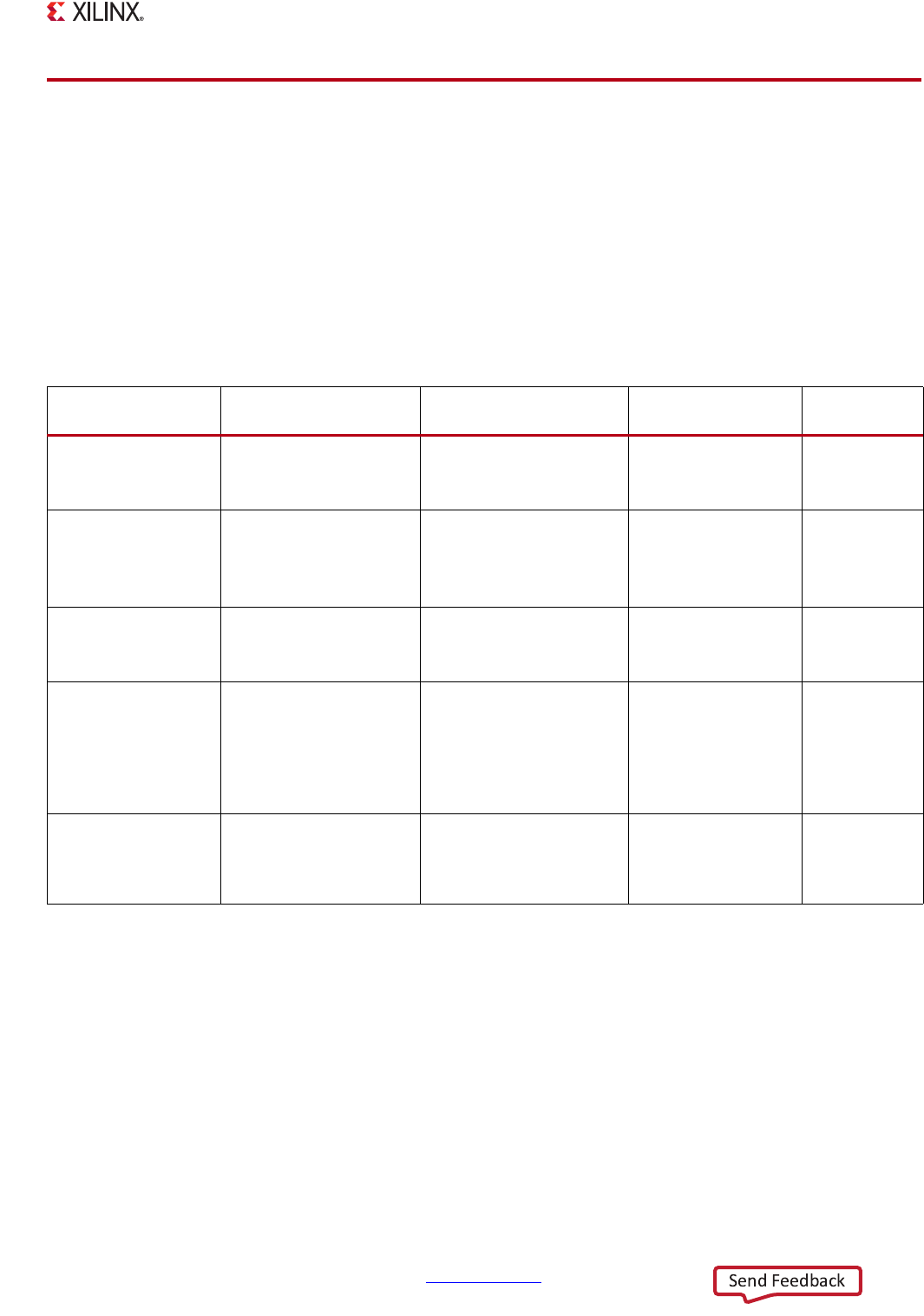
Table 22-8: Data Movement Method Comparison Summary
Method Benefits Drawbacks Suggested Uses
Estimated
Throughput
CPU Programmed I/O • Simple Software
• Least PL Resources
• Simple PL Slaves
• Lowest Throughput • Control Functions <25 MB/s
PS DMAC • Least PL Resources
• Medium Throughput
• Multiple Channels
• Simple PL Slaves
•Somewhat complex
DMA programming
• Limited PL
Resource DMAs
600 MB/s
PL AXI_HP DMA • Highest Throughput
•Multiple Interfaces
• Command/Data FIFOs
• OCM/DDR access only
•More complex PL
Master design
• High Performance
DMA for large
datasets
1,200 MB/s
(per interface)
PL AXI_ACP DMA • Highest Throughput
• Lowest Latency
• Optional Cache
Coherency
•Large burst might cause
cache thrashing
•Shares CPU
Interconnect bandwidth
•More complex PL
Master design
• High Performance
DMA for smaller,
coherent datasets
•Medium
granularity CPU
offload
1,200 MB/s
PL AXI_GP DMA • Medium Throughput • More complex PL
Master design
•PL to PS Control
Functions
•PS I/O Peripheral
Access
600 MB/s