
User manual


Table Of Contents
- Zynq-7000 All Programmable SoC
- Table of Contents
- Ch. 1: Introduction
- Ch. 2: Signals, Interfaces, and Pins
- Ch. 3: Application Processing Unit
- Ch. 4: System Addresses
- Ch. 5: Interconnect
- Ch. 6: Boot and Configuration
- Ch. 7: Interrupts
- Ch. 8: Timers
- Ch. 9: DMA Controller
- Introduction
- Functional Description
- DMA Transfers on the AXI Interconnect
- AXI Transaction Considerations
- DMA Manager
- Multi-channel Data FIFO (MFIFO)
- Memory-to-Memory Transfers
- PL Peripheral AXI Transactions
- PL Peripheral Request Interface
- PL Peripheral - Length Managed by PL Peripheral
- PL Peripheral - Length Managed by DMAC
- Events and Interrupts
- Aborts
- Security
- IP Configuration Options
- Programming Guide for DMA Controller
- Programming Guide for DMA Engine
- Programming Restrictions
- System Functions
- I/O Interface
- Ch. 10: DDR Memory Controller
- Introduction
- AXI Memory Port Interface (DDRI)
- DDR Core and Transaction Scheduler (DDRC)
- DDRC Arbitration
- Controller PHY (DDRP)
- Initialization and Calibration
- DDR Clock Initialization
- DDR IOB Impedance Calibration
- DDR IOB Configuration
- DDR Controller Register Programming
- DRAM Reset and Initialization
- DRAM Input Impedance (ODT) Calibration
- DRAM Output Impedance (RON) Calibration
- DRAM Training
- Write Data Eye Adjustment
- Alternatives to Automatic DRAM Training
- DRAM Write Latency Restriction
- Register Overview
- Error Correction Code (ECC)
- Programming Model
- Ch. 11: Static Memory Controller
- Ch. 12: Quad-SPI Flash Controller
- Ch. 13: SD/SDIO Controller
- Ch. 14: General Purpose I/O (GPIO)
- Ch. 15: USB Host, Device, and OTG Controller
- Introduction
- Functional Description
- Programming Overview and Reference
- Device Mode Control
- Device Endpoint Data Structures
- Device Endpoint Packet Operational Model
- Device Endpoint Descriptor Reference
- Programming Guide for Device Controller
- Programming Guide for Device Endpoint Data Structures
- Host Mode Data Structures
- EHCI Implementation
- Host Data Structures Reference
- Programming Guide for Host Controller
- OTG Description and Reference
- System Functions
- I/O Interfaces
- Ch. 16: Gigabit Ethernet Controller
- Ch. 17: SPI Controller
- Ch. 18: CAN Controller
- Ch. 19: UART Controller
- Ch. 20: I2C Controller
- Ch. 21: Programmable Logic Description
- Ch. 22: Programmable Logic Design Guide
- Ch. 23: Programmable Logic Test and Debug
- Ch. 24: Power Management
- Ch. 25: Clocks
- Ch. 26: Reset System
- Ch. 27: JTAG and DAP Subsystem
- Ch. 28: System Test and Debug
- Ch. 29: On-Chip Memory (OCM)
- Ch. 30: XADC Interface
- Ch. 31: PCI Express
- Ch. 32: Device Secure Boot
- Appx. A: Additional Resources
- Appx. B: Register Details
- Overview
- Acronyms
- Module Summary
- AXI_HP Interface (AFI) (axi_hp)
- CAN Controller (can)
- DDR Memory Controller (ddrc)
- CoreSight Cross Trigger Interface (cti)
- Performance Monitor Unit (cortexa9_pmu)
- CoreSight Program Trace Macrocell (ptm)
- Debug Access Port (dap)
- CoreSight Embedded Trace Buffer (etb)
- PL Fabric Trace Monitor (ftm)
- CoreSight Trace Funnel (funnel)
- CoreSight Intstrumentation Trace Macrocell (itm)
- CoreSight Trace Packet Output (tpiu)
- Device Configuration Interface (devcfg)
- DMA Controller (dmac)
- Gigabit Ethernet Controller (GEM)
- General Purpose I/O (gpio)
- Interconnect QoS (qos301)
- NIC301 Address Region Control (nic301_addr_region_ctrl_registers)
- I2C Controller (IIC)
- L2 Cache (L2Cpl310)
- Application Processing Unit (mpcore)
- On-Chip Memory (ocm)
- Quad-SPI Flash Controller (qspi)
- SD Controller (sdio)
- System Level Control Registers (slcr)
- Static Memory Controller (pl353)
- SPI Controller (SPI)
- System Watchdog Timer (swdt)
- Triple Timer Counter (ttc)
- UART Controller (UART)
- USB Controller (usb)
Zynq-7000 AP SoC Technical Reference Manual www.xilinx.com 656
UG585 (v1.11) September 27, 2016
Chapter 22: Programmable Logic Design Guide
Drawbacks of using a CPU to move data is that a sophisticated CPU is spending cycles performing
simple data movement instead of complex control and computation tasks, and the limited
throughput available. Transfer rates less than 25 MB/s are reasonable with this method.
22.4.3 PS DMA Controller (DMAC) via General Purpose Masters
The PS DMA controller (DMAC) provides a flexible DMA engine that can provide moderate levels of
throughput with little PL logic resource usage (see Figure 22-2). The DMAC resides in the PS and
must be programmed via DMA instructions residing in memory, typically prepared by a CPU. With
support for up to eight channels, multiple DMA fabric cores can potentially be served in the single
DMAC. However, the flexible programmable model might increase software complexity relative to
CPU transfer or specialized PL DMA.
The DMAC interface to the PL is through the general purpose AXI master interfaces, whose 32-bit
width along with the centralized DMA nature (a read and write transaction for each movement) of the
DMAC to limit the DMAC from highest throughput. A peripheral request interface also allows PL
slaves to provide status to the DMAC on buffer state, to prevent transactions involving a stalled PL
peripheral from unnecessarily also stalling interconnect and DMAC bandwidth.
See Chapter 9, DMA Controller for more information on the DMAC controller. More information on
the M_AXI_GP interfaces can be found in Chapter 5, Interconnect.
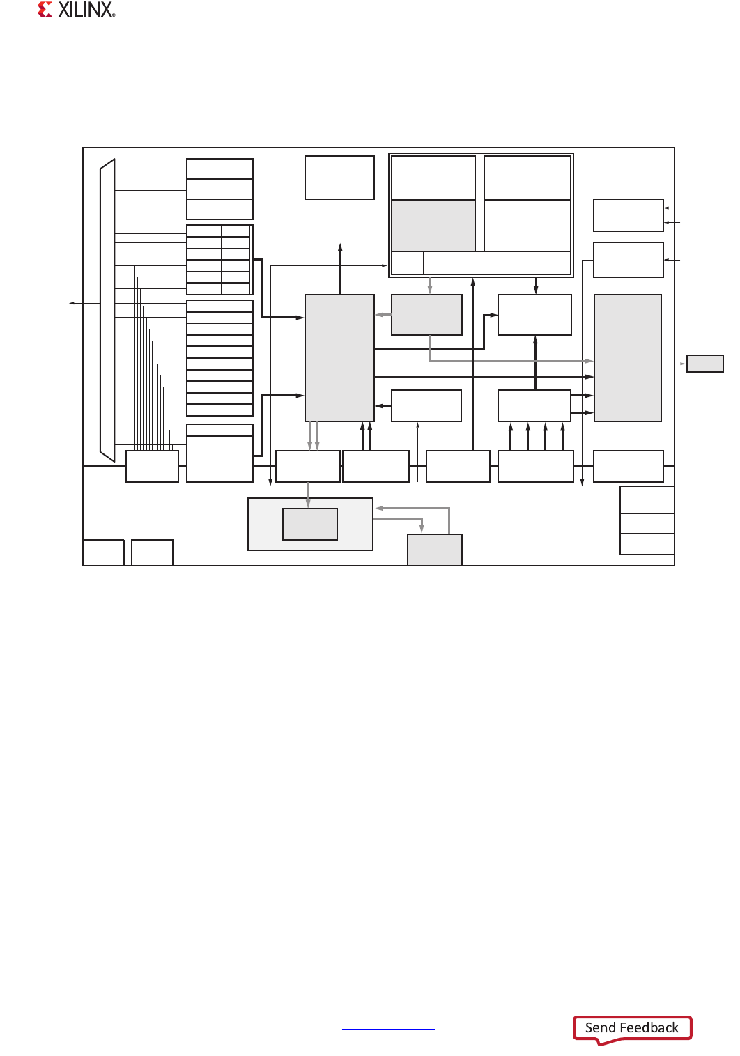
X-Ref Target - Figure 22-1
Figure 22-1: Example Cortex-A9 PL Data Movement Topology
IRQ
L2
Cache Memory
512 KB
DDR
Memory
Controller
16-bit
32-bit
16-bit w/ECC
DMA
8 channel
PCAP
Processor Config
Access Port
M_AXI_GP x 2
General Purpose
32-bit AXI Master
S_AXI_GP x 2
General Purpose
32-bit AXI Slave
S_AXI_HP x 4
AXI Data
32/64-bit Slave
SCU – Snoop Control Unit
Central
Interconnect
ARM A9
32 KB I-Cache
32 KB D-Cache
NEON
SP, DP FPU
128-bit Vector DSP
OCM
On Chip Memory
256 KB
S_AXI_ACP
AXI Coherent
64-bit Slave
Mem Switch
SLCR
System Level
Control
Registers
I/O Interface
Security
Config
XADC
16 ch ADC
Block RAM
User
IP
PCIe
Quad-SPI
1,2,4,8-bit
Parallel 8-bit
NOR/SRAM
NAND 8,16-bit
UART
UART
SPI
SPI
I2C
I2C
CAN
CAN
TTC/SWDT
PJTAG
Reset
CLK / PLL
ARM, I/O, DDR
PS_POR_B
PS_SRST_B
PS_CLK
DDR
CoreSight
Trace In
Trace Out
Cross Trigger
DAP
APB
Register Access
Processing
System (PS)
EMIO
USB
USB
GigE
GigE
SD
SD
DMA
DMA
DMA
DMA
DMA
DMA
GPIO x54, x64
MIO
Pins
GTX or
GTP
NEON
SP, DP FPU
128-bit Vector DSP
ARM A9
32 KB I-Cache
32 KB D-Cache
UG585_c22_03_102414
Programmable
Logic (PL)
NOTE: GigaBit Transceiver and PCIe
functionality are not available in
all device versions and packages.