
User manual


Table Of Contents
- Zynq-7000 All Programmable SoC
- Table of Contents
- Ch. 1: Introduction
- Ch. 2: Signals, Interfaces, and Pins
- Ch. 3: Application Processing Unit
- Ch. 4: System Addresses
- Ch. 5: Interconnect
- Ch. 6: Boot and Configuration
- Ch. 7: Interrupts
- Ch. 8: Timers
- Ch. 9: DMA Controller
- Introduction
- Functional Description
- DMA Transfers on the AXI Interconnect
- AXI Transaction Considerations
- DMA Manager
- Multi-channel Data FIFO (MFIFO)
- Memory-to-Memory Transfers
- PL Peripheral AXI Transactions
- PL Peripheral Request Interface
- PL Peripheral - Length Managed by PL Peripheral
- PL Peripheral - Length Managed by DMAC
- Events and Interrupts
- Aborts
- Security
- IP Configuration Options
- Programming Guide for DMA Controller
- Programming Guide for DMA Engine
- Programming Restrictions
- System Functions
- I/O Interface
- Ch. 10: DDR Memory Controller
- Introduction
- AXI Memory Port Interface (DDRI)
- DDR Core and Transaction Scheduler (DDRC)
- DDRC Arbitration
- Controller PHY (DDRP)
- Initialization and Calibration
- DDR Clock Initialization
- DDR IOB Impedance Calibration
- DDR IOB Configuration
- DDR Controller Register Programming
- DRAM Reset and Initialization
- DRAM Input Impedance (ODT) Calibration
- DRAM Output Impedance (RON) Calibration
- DRAM Training
- Write Data Eye Adjustment
- Alternatives to Automatic DRAM Training
- DRAM Write Latency Restriction
- Register Overview
- Error Correction Code (ECC)
- Programming Model
- Ch. 11: Static Memory Controller
- Ch. 12: Quad-SPI Flash Controller
- Ch. 13: SD/SDIO Controller
- Ch. 14: General Purpose I/O (GPIO)
- Ch. 15: USB Host, Device, and OTG Controller
- Introduction
- Functional Description
- Programming Overview and Reference
- Device Mode Control
- Device Endpoint Data Structures
- Device Endpoint Packet Operational Model
- Device Endpoint Descriptor Reference
- Programming Guide for Device Controller
- Programming Guide for Device Endpoint Data Structures
- Host Mode Data Structures
- EHCI Implementation
- Host Data Structures Reference
- Programming Guide for Host Controller
- OTG Description and Reference
- System Functions
- I/O Interfaces
- Ch. 16: Gigabit Ethernet Controller
- Ch. 17: SPI Controller
- Ch. 18: CAN Controller
- Ch. 19: UART Controller
- Ch. 20: I2C Controller
- Ch. 21: Programmable Logic Description
- Ch. 22: Programmable Logic Design Guide
- Ch. 23: Programmable Logic Test and Debug
- Ch. 24: Power Management
- Ch. 25: Clocks
- Ch. 26: Reset System
- Ch. 27: JTAG and DAP Subsystem
- Ch. 28: System Test and Debug
- Ch. 29: On-Chip Memory (OCM)
- Ch. 30: XADC Interface
- Ch. 31: PCI Express
- Ch. 32: Device Secure Boot
- Appx. A: Additional Resources
- Appx. B: Register Details
- Overview
- Acronyms
- Module Summary
- AXI_HP Interface (AFI) (axi_hp)
- CAN Controller (can)
- DDR Memory Controller (ddrc)
- CoreSight Cross Trigger Interface (cti)
- Performance Monitor Unit (cortexa9_pmu)
- CoreSight Program Trace Macrocell (ptm)
- Debug Access Port (dap)
- CoreSight Embedded Trace Buffer (etb)
- PL Fabric Trace Monitor (ftm)
- CoreSight Trace Funnel (funnel)
- CoreSight Intstrumentation Trace Macrocell (itm)
- CoreSight Trace Packet Output (tpiu)
- Device Configuration Interface (devcfg)
- DMA Controller (dmac)
- Gigabit Ethernet Controller (GEM)
- General Purpose I/O (gpio)
- Interconnect QoS (qos301)
- NIC301 Address Region Control (nic301_addr_region_ctrl_registers)
- I2C Controller (IIC)
- L2 Cache (L2Cpl310)
- Application Processing Unit (mpcore)
- On-Chip Memory (ocm)
- Quad-SPI Flash Controller (qspi)
- SD Controller (sdio)
- System Level Control Registers (slcr)
- Static Memory Controller (pl353)
- SPI Controller (SPI)
- System Watchdog Timer (swdt)
- Triple Timer Counter (ttc)
- UART Controller (UART)
- USB Controller (usb)
Zynq-7000 AP SoC Technical Reference Manual www.xilinx.com 668
UG585 (v1.11) September 27, 2016
Chapter 23: Programmable Logic Test and Debug
23.3.2 Trigger Signals
23.3.3 Trace Signals
General purpose
debug input
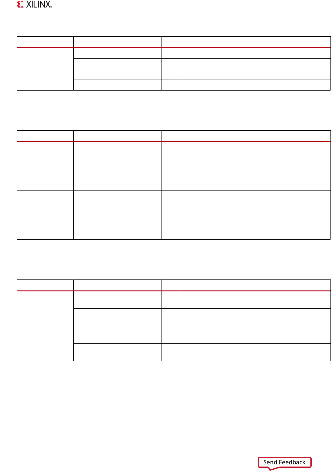
FTMTF2PDEBUG[7:0] I The FTMF2PDBG0 register shows its value.
FTMTF2PDEBUG[15:8] I The FTMF2PDBG1 register shows its value.
FTMTF2PDEBUG[23:16] I The FTMF2PDBG2 register shows its value.
FTMTF2PDEBUG[31:24] I The FTMF2PDBG3 register shows its value.
Table 23-8: General-Purpose Debug Signals
Group PS-PL Signal IO Description
Table 23-9: Trigger Signals
Group PS-PL Signal IO Description
Trigger from
PS to PL
FTMTP2FTRIG[3:0] O
Each bit is an asynchronous trigger signal from the
CoreSight ECT structure in the PS to the PL. Users must
program the CTI connected to the FTM to enable these
trigger output signals.
FTMTP2FTRIGACK[3:0] I
Each bit is the asynchronous acknowledge signal for the
corresponding FTMTP2FTRIG signal.
Trigger from
PL to PS
FTMTF2PTRIG[3:0] I
Each bit is an asynchronous trigger signal from the PL
to the CoreSight ECT structure in the PS. Users must
program the CTI connected to FTM to enable these
trigger input signals.
FTMTF2PTRIGACK[3:0] O
Each bit is the asynchronous acknowledge signal for the
corresponding FTMTF2PTRIG signal.
Table 23-10: Trace Signals
Group PS-PL Signal IO Description
Trace from
PL to PS
FTMDTRACEINCLOCK I
Clock signal for the trace data interface. Asynchronous
to the PS.
FTMDTRACEINVALID I
When this signal is sampled High by the PS using
FTMDTRACEINCLOCK, the values on
TRMDTRACEINDATA and FTMDTRACEINATID are valid.
FTMDTRACEINDATA[31:0] I Trace data. All 32 bits must be provided.
FTMDTRACEINATID[3:0] I
Trace ID to be carried over to the ATB. All 4 bits must be
provided.