
User manual


Table Of Contents
- Zynq-7000 All Programmable SoC
- Table of Contents
- Ch. 1: Introduction
- Ch. 2: Signals, Interfaces, and Pins
- Ch. 3: Application Processing Unit
- Ch. 4: System Addresses
- Ch. 5: Interconnect
- Ch. 6: Boot and Configuration
- Ch. 7: Interrupts
- Ch. 8: Timers
- Ch. 9: DMA Controller
- Introduction
- Functional Description
- DMA Transfers on the AXI Interconnect
- AXI Transaction Considerations
- DMA Manager
- Multi-channel Data FIFO (MFIFO)
- Memory-to-Memory Transfers
- PL Peripheral AXI Transactions
- PL Peripheral Request Interface
- PL Peripheral - Length Managed by PL Peripheral
- PL Peripheral - Length Managed by DMAC
- Events and Interrupts
- Aborts
- Security
- IP Configuration Options
- Programming Guide for DMA Controller
- Programming Guide for DMA Engine
- Programming Restrictions
- System Functions
- I/O Interface
- Ch. 10: DDR Memory Controller
- Introduction
- AXI Memory Port Interface (DDRI)
- DDR Core and Transaction Scheduler (DDRC)
- DDRC Arbitration
- Controller PHY (DDRP)
- Initialization and Calibration
- DDR Clock Initialization
- DDR IOB Impedance Calibration
- DDR IOB Configuration
- DDR Controller Register Programming
- DRAM Reset and Initialization
- DRAM Input Impedance (ODT) Calibration
- DRAM Output Impedance (RON) Calibration
- DRAM Training
- Write Data Eye Adjustment
- Alternatives to Automatic DRAM Training
- DRAM Write Latency Restriction
- Register Overview
- Error Correction Code (ECC)
- Programming Model
- Ch. 11: Static Memory Controller
- Ch. 12: Quad-SPI Flash Controller
- Ch. 13: SD/SDIO Controller
- Ch. 14: General Purpose I/O (GPIO)
- Ch. 15: USB Host, Device, and OTG Controller
- Introduction
- Functional Description
- Programming Overview and Reference
- Device Mode Control
- Device Endpoint Data Structures
- Device Endpoint Packet Operational Model
- Device Endpoint Descriptor Reference
- Programming Guide for Device Controller
- Programming Guide for Device Endpoint Data Structures
- Host Mode Data Structures
- EHCI Implementation
- Host Data Structures Reference
- Programming Guide for Host Controller
- OTG Description and Reference
- System Functions
- I/O Interfaces
- Ch. 16: Gigabit Ethernet Controller
- Ch. 17: SPI Controller
- Ch. 18: CAN Controller
- Ch. 19: UART Controller
- Ch. 20: I2C Controller
- Ch. 21: Programmable Logic Description
- Ch. 22: Programmable Logic Design Guide
- Ch. 23: Programmable Logic Test and Debug
- Ch. 24: Power Management
- Ch. 25: Clocks
- Ch. 26: Reset System
- Ch. 27: JTAG and DAP Subsystem
- Ch. 28: System Test and Debug
- Ch. 29: On-Chip Memory (OCM)
- Ch. 30: XADC Interface
- Ch. 31: PCI Express
- Ch. 32: Device Secure Boot
- Appx. A: Additional Resources
- Appx. B: Register Details
- Overview
- Acronyms
- Module Summary
- AXI_HP Interface (AFI) (axi_hp)
- CAN Controller (can)
- DDR Memory Controller (ddrc)
- CoreSight Cross Trigger Interface (cti)
- Performance Monitor Unit (cortexa9_pmu)
- CoreSight Program Trace Macrocell (ptm)
- Debug Access Port (dap)
- CoreSight Embedded Trace Buffer (etb)
- PL Fabric Trace Monitor (ftm)
- CoreSight Trace Funnel (funnel)
- CoreSight Intstrumentation Trace Macrocell (itm)
- CoreSight Trace Packet Output (tpiu)
- Device Configuration Interface (devcfg)
- DMA Controller (dmac)
- Gigabit Ethernet Controller (GEM)
- General Purpose I/O (gpio)
- Interconnect QoS (qos301)
- NIC301 Address Region Control (nic301_addr_region_ctrl_registers)
- I2C Controller (IIC)
- L2 Cache (L2Cpl310)
- Application Processing Unit (mpcore)
- On-Chip Memory (ocm)
- Quad-SPI Flash Controller (qspi)
- SD Controller (sdio)
- System Level Control Registers (slcr)
- Static Memory Controller (pl353)
- SPI Controller (SPI)
- System Watchdog Timer (swdt)
- Triple Timer Counter (ttc)
- UART Controller (UART)
- USB Controller (usb)
Zynq-7000 AP SoC Technical Reference Manual www.xilinx.com 680
UG585 (v1.11) September 27, 2016
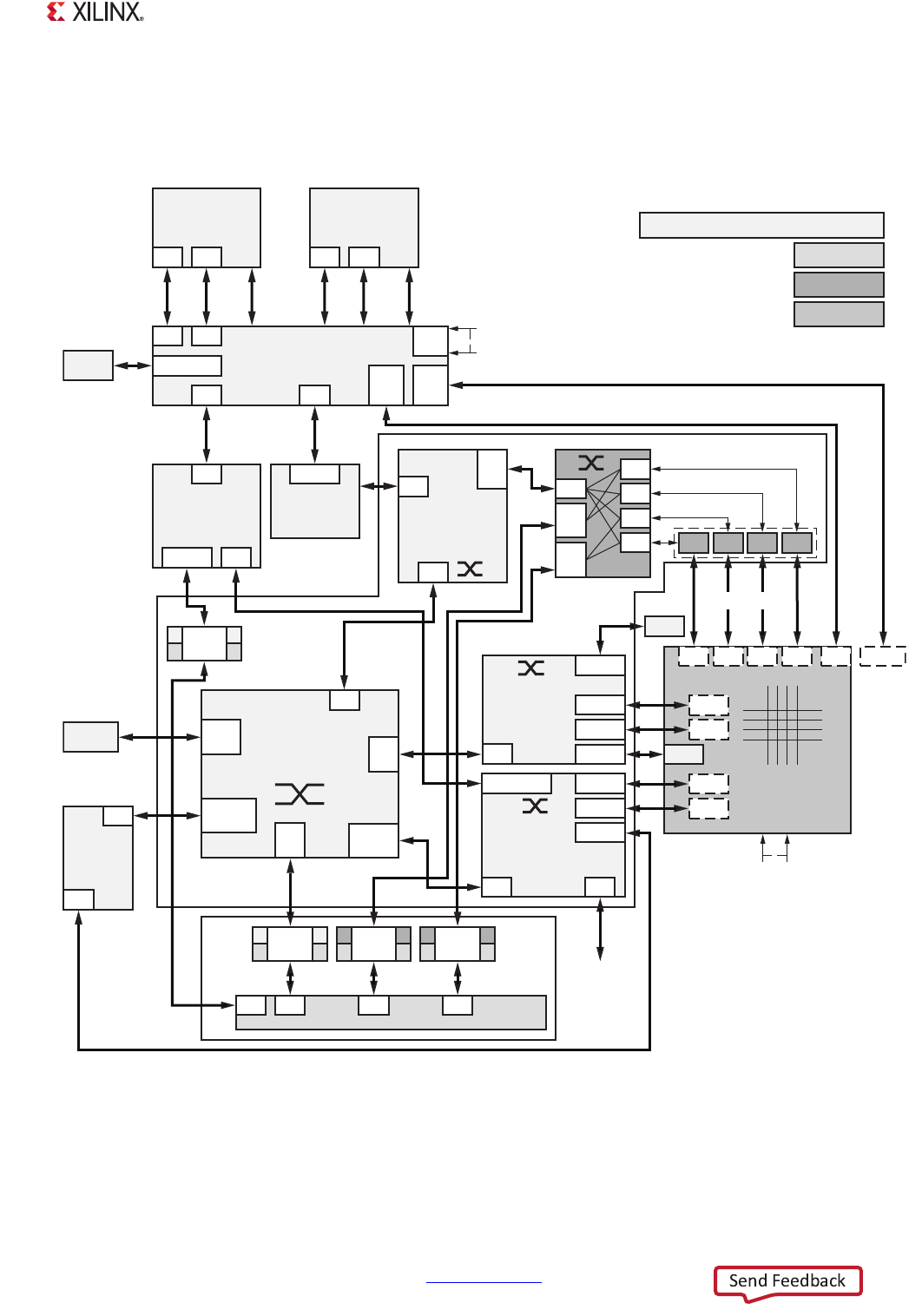
Chapter 25: Clocks
25.1.3 System Viewpoint
Figure 25-1 shows the clock network and related domains from a system viewpoint.
X-Ref Target - Figure 25-2
Figure 25-2: System Clock Domains
UG585_c25_02_021213
A9 MP Core
TAG
32K I-Cache
32L D-Cache
M0
DMAC
M1
L-2 Cache
Controller
Snoop Control
Unit (SCU)
512 KB Cache
M0 AS M1
S0
TAG CTRL
S1
GIC
Peripheral +
PL Interrupts
EVENT
AS: Async Domain
US: Up Sync
DS: Down Sync
UZ: Up Size
DZ: Down Size
ACP
EVT
ACP
AXI
M1
AFI AFI AFI AFI
M0 M1 M2 M3
M0
M0
S0
OCM
Interconnect
64-bit
CPU_2x
M2
S3
S2
S1
S0
M1
US
M0
US
s1
S0
AS
256 KB OCM
RAM
S0 DS
M0 Event
I-AXI D-AXI Coherent
A9 MP Core
PL
32K I-Cache
32L D-Cache
M0 M1
I-AXI
D-AXI Coherent
Master
Interconnect
32-Bit
CPU_2x
M0
S0 US
S1 AS
S2 AS
DAP
DVC
M1
M0
S3 US
Slave
Interconnect
32-Bit
CPU_2x
M3
S0
M0 ASS1 DS/DZ
M1 AS
M2 DS
Central
Interconnect
(3x3)
64-Bit CPU_2x
Top Bus
Switch
DDR
Controller
M0
M1
DS/DZ
Async
Bridge
S0 QoS
US/UZ
S2
QoS
M2
AS
Async
Bridge
Async
Bridge
S1
UZ
S0
S1
Peripheral
Interrupts
Peripheral
APB
S1S0 S2 S3
Async
QoS
M0
S0
IOP
32-Bit
CPU_1x
DDR 3X CLK
CPU CLK (CPU_6x, CPU_2x, and CPU_1x)
DDR 2X CLK
FPGA CLKs
AXI_HP 64/32