
User manual


Table Of Contents
- Zynq-7000 All Programmable SoC
- Table of Contents
- Ch. 1: Introduction
- Ch. 2: Signals, Interfaces, and Pins
- Ch. 3: Application Processing Unit
- Ch. 4: System Addresses
- Ch. 5: Interconnect
- Ch. 6: Boot and Configuration
- Ch. 7: Interrupts
- Ch. 8: Timers
- Ch. 9: DMA Controller
- Introduction
- Functional Description
- DMA Transfers on the AXI Interconnect
- AXI Transaction Considerations
- DMA Manager
- Multi-channel Data FIFO (MFIFO)
- Memory-to-Memory Transfers
- PL Peripheral AXI Transactions
- PL Peripheral Request Interface
- PL Peripheral - Length Managed by PL Peripheral
- PL Peripheral - Length Managed by DMAC
- Events and Interrupts
- Aborts
- Security
- IP Configuration Options
- Programming Guide for DMA Controller
- Programming Guide for DMA Engine
- Programming Restrictions
- System Functions
- I/O Interface
- Ch. 10: DDR Memory Controller
- Introduction
- AXI Memory Port Interface (DDRI)
- DDR Core and Transaction Scheduler (DDRC)
- DDRC Arbitration
- Controller PHY (DDRP)
- Initialization and Calibration
- DDR Clock Initialization
- DDR IOB Impedance Calibration
- DDR IOB Configuration
- DDR Controller Register Programming
- DRAM Reset and Initialization
- DRAM Input Impedance (ODT) Calibration
- DRAM Output Impedance (RON) Calibration
- DRAM Training
- Write Data Eye Adjustment
- Alternatives to Automatic DRAM Training
- DRAM Write Latency Restriction
- Register Overview
- Error Correction Code (ECC)
- Programming Model
- Ch. 11: Static Memory Controller
- Ch. 12: Quad-SPI Flash Controller
- Ch. 13: SD/SDIO Controller
- Ch. 14: General Purpose I/O (GPIO)
- Ch. 15: USB Host, Device, and OTG Controller
- Introduction
- Functional Description
- Programming Overview and Reference
- Device Mode Control
- Device Endpoint Data Structures
- Device Endpoint Packet Operational Model
- Device Endpoint Descriptor Reference
- Programming Guide for Device Controller
- Programming Guide for Device Endpoint Data Structures
- Host Mode Data Structures
- EHCI Implementation
- Host Data Structures Reference
- Programming Guide for Host Controller
- OTG Description and Reference
- System Functions
- I/O Interfaces
- Ch. 16: Gigabit Ethernet Controller
- Ch. 17: SPI Controller
- Ch. 18: CAN Controller
- Ch. 19: UART Controller
- Ch. 20: I2C Controller
- Ch. 21: Programmable Logic Description
- Ch. 22: Programmable Logic Design Guide
- Ch. 23: Programmable Logic Test and Debug
- Ch. 24: Power Management
- Ch. 25: Clocks
- Ch. 26: Reset System
- Ch. 27: JTAG and DAP Subsystem
- Ch. 28: System Test and Debug
- Ch. 29: On-Chip Memory (OCM)
- Ch. 30: XADC Interface
- Ch. 31: PCI Express
- Ch. 32: Device Secure Boot
- Appx. A: Additional Resources
- Appx. B: Register Details
- Overview
- Acronyms
- Module Summary
- AXI_HP Interface (AFI) (axi_hp)
- CAN Controller (can)
- DDR Memory Controller (ddrc)
- CoreSight Cross Trigger Interface (cti)
- Performance Monitor Unit (cortexa9_pmu)
- CoreSight Program Trace Macrocell (ptm)
- Debug Access Port (dap)
- CoreSight Embedded Trace Buffer (etb)
- PL Fabric Trace Monitor (ftm)
- CoreSight Trace Funnel (funnel)
- CoreSight Intstrumentation Trace Macrocell (itm)
- CoreSight Trace Packet Output (tpiu)
- Device Configuration Interface (devcfg)
- DMA Controller (dmac)
- Gigabit Ethernet Controller (GEM)
- General Purpose I/O (gpio)
- Interconnect QoS (qos301)
- NIC301 Address Region Control (nic301_addr_region_ctrl_registers)
- I2C Controller (IIC)
- L2 Cache (L2Cpl310)
- Application Processing Unit (mpcore)
- On-Chip Memory (ocm)
- Quad-SPI Flash Controller (qspi)
- SD Controller (sdio)
- System Level Control Registers (slcr)
- Static Memory Controller (pl353)
- SPI Controller (SPI)
- System Watchdog Timer (swdt)
- Triple Timer Counter (ttc)
- UART Controller (UART)
- USB Controller (usb)
Zynq-7000 AP SoC Technical Reference Manual www.xilinx.com 682
UG585 (v1.11) September 27, 2016
Chapter 25: Clocks
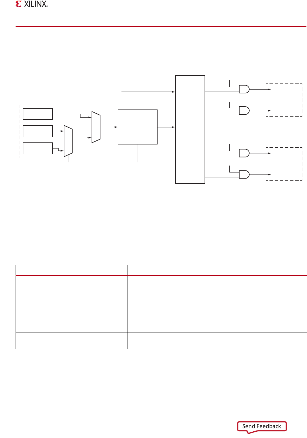
25.2 CPU Clock
Figure 25-3 shows the clock generation network in the CPU clock domains.
Ratio Examples
The CPU clock domain operates in two modes 6:2:1 and 4:2:1. Table 25-1 shows example frequencies
for these modes and modules operating in each clock domain. (See the applicable Zynq-7000 AP SoC
data sheet for the specific allowed frequencies for each clock.)
CPU Clock Divisor Restriction
To improve the quality of the high speed clocks going to the CPU and DDR, there is a requirement
that they get divided by an even number in the slcr.ARM_CLK_CTRL [DIVISOR] bit field. For the
slcr.ARM_CLK_CTRL [DIVISOR], software must program the following values: DIVISOR =2, =4, or >4.
X-Ref Target - Figure 25-3
Figure 25-3: CPU Clock Generation and Domains
UG585_c25_03_022912
ARM PLL
DDR PLL
IO PLL
[5][4]
6-bit
Programmable
Divider
[13:8]
ARM_CLK_CTRL
ARM_CLK_CTRL
ARM_CLK_CTRL [24]
CPU_6x4x
Glitch-
Free
Glitch-Free
Glitch-
Free
Glitch-
Free
1
0
1
0
1
Clock
Ratio
Generator
ARM_CLK_CTRL [25]
Closely Coupled,
Always 2:1 Ratio
CPU_3x2x
2:1
ARM_CLK_CTRL [26]
CPU_2x
2:1 or 3:1
ARM_CLK_CTRL [27]
Closely Coupled,
Always 2:1 Ratio
CPU_1x
6:1 or 4:1
CLK_621_TRUE [0]
Table 25-1: CPU Clock Frequency Ratio Examples
CPU Clock 6:2:1 4:2:1 Clock Domain Modules
CPU_6x4x 800 MHz
(6 times faster than CPU_1x)
600 MHz
(4 times faster than CPU_1x)
CPU clock frequency, SCU, and OCM
arbitration, NEON, L2 cache memory
CPU_3x2x 400 MHz
(3 times faster than CPU_1x)
300 MHz
(2 times faster than CPU_1x)
APU timers
CPU_2x 266 MHz
(2 times faster than CPU_1x)
300 MHz
(2 times faster than CPU_1x)
I/O peripherals, central interconnect,
master interconnect, slave interconnect,
and OCM RAM
CPU_1x 133 MHz 150 MHz I/O peripherals AHB and APB interface
busses