
User manual


Table Of Contents
- Zynq-7000 All Programmable SoC
- Table of Contents
- Ch. 1: Introduction
- Ch. 2: Signals, Interfaces, and Pins
- Ch. 3: Application Processing Unit
- Ch. 4: System Addresses
- Ch. 5: Interconnect
- Ch. 6: Boot and Configuration
- Ch. 7: Interrupts
- Ch. 8: Timers
- Ch. 9: DMA Controller
- Introduction
- Functional Description
- DMA Transfers on the AXI Interconnect
- AXI Transaction Considerations
- DMA Manager
- Multi-channel Data FIFO (MFIFO)
- Memory-to-Memory Transfers
- PL Peripheral AXI Transactions
- PL Peripheral Request Interface
- PL Peripheral - Length Managed by PL Peripheral
- PL Peripheral - Length Managed by DMAC
- Events and Interrupts
- Aborts
- Security
- IP Configuration Options
- Programming Guide for DMA Controller
- Programming Guide for DMA Engine
- Programming Restrictions
- System Functions
- I/O Interface
- Ch. 10: DDR Memory Controller
- Introduction
- AXI Memory Port Interface (DDRI)
- DDR Core and Transaction Scheduler (DDRC)
- DDRC Arbitration
- Controller PHY (DDRP)
- Initialization and Calibration
- DDR Clock Initialization
- DDR IOB Impedance Calibration
- DDR IOB Configuration
- DDR Controller Register Programming
- DRAM Reset and Initialization
- DRAM Input Impedance (ODT) Calibration
- DRAM Output Impedance (RON) Calibration
- DRAM Training
- Write Data Eye Adjustment
- Alternatives to Automatic DRAM Training
- DRAM Write Latency Restriction
- Register Overview
- Error Correction Code (ECC)
- Programming Model
- Ch. 11: Static Memory Controller
- Ch. 12: Quad-SPI Flash Controller
- Ch. 13: SD/SDIO Controller
- Ch. 14: General Purpose I/O (GPIO)
- Ch. 15: USB Host, Device, and OTG Controller
- Introduction
- Functional Description
- Programming Overview and Reference
- Device Mode Control
- Device Endpoint Data Structures
- Device Endpoint Packet Operational Model
- Device Endpoint Descriptor Reference
- Programming Guide for Device Controller
- Programming Guide for Device Endpoint Data Structures
- Host Mode Data Structures
- EHCI Implementation
- Host Data Structures Reference
- Programming Guide for Host Controller
- OTG Description and Reference
- System Functions
- I/O Interfaces
- Ch. 16: Gigabit Ethernet Controller
- Ch. 17: SPI Controller
- Ch. 18: CAN Controller
- Ch. 19: UART Controller
- Ch. 20: I2C Controller
- Ch. 21: Programmable Logic Description
- Ch. 22: Programmable Logic Design Guide
- Ch. 23: Programmable Logic Test and Debug
- Ch. 24: Power Management
- Ch. 25: Clocks
- Ch. 26: Reset System
- Ch. 27: JTAG and DAP Subsystem
- Ch. 28: System Test and Debug
- Ch. 29: On-Chip Memory (OCM)
- Ch. 30: XADC Interface
- Ch. 31: PCI Express
- Ch. 32: Device Secure Boot
- Appx. A: Additional Resources
- Appx. B: Register Details
- Overview
- Acronyms
- Module Summary
- AXI_HP Interface (AFI) (axi_hp)
- CAN Controller (can)
- DDR Memory Controller (ddrc)
- CoreSight Cross Trigger Interface (cti)
- Performance Monitor Unit (cortexa9_pmu)
- CoreSight Program Trace Macrocell (ptm)
- Debug Access Port (dap)
- CoreSight Embedded Trace Buffer (etb)
- PL Fabric Trace Monitor (ftm)
- CoreSight Trace Funnel (funnel)
- CoreSight Intstrumentation Trace Macrocell (itm)
- CoreSight Trace Packet Output (tpiu)
- Device Configuration Interface (devcfg)
- DMA Controller (dmac)
- Gigabit Ethernet Controller (GEM)
- General Purpose I/O (gpio)
- Interconnect QoS (qos301)
- NIC301 Address Region Control (nic301_addr_region_ctrl_registers)
- I2C Controller (IIC)
- L2 Cache (L2Cpl310)
- Application Processing Unit (mpcore)
- On-Chip Memory (ocm)
- Quad-SPI Flash Controller (qspi)
- SD Controller (sdio)
- System Level Control Registers (slcr)
- Static Memory Controller (pl353)
- SPI Controller (SPI)
- System Watchdog Timer (swdt)
- Triple Timer Counter (ttc)
- UART Controller (UART)
- USB Controller (usb)
Zynq-7000 AP SoC Technical Reference Manual www.xilinx.com 685
UG585 (v1.11) September 27, 2016
Chapter 25: Clocks
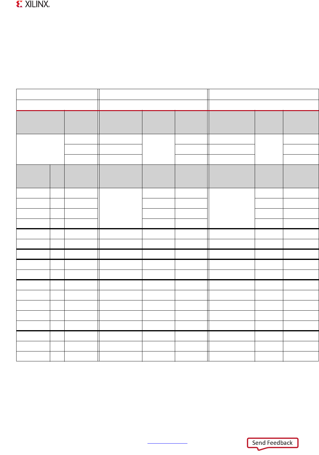
The PLL output frequency is determined by the frequency of the input clock PS_CLK multiplied by the
PLL feedback divider value (M value). The example below assumes the ARM PLL feedback divider
value is 40, which generates an ARM PLL output frequency of 33.33 MHz * 40 = 1.33 GHz. For each
of the clocks listed in the lower half of the table, the clock frequency equals the sourced PLL
frequency divided by the divisor value. For some of the peripheral clocks, such as CAN, Ethernet, and
the PL, there are two cascaded dividers.
Table 25-3: Clock Frequency Setting Examples for 6:2:1 Mode
Example 1 Example 2
PS_CLK 33.33 MHz 50 MHz
PLL PLL Feedback
Divider Value
PLL Output
Frequency
(MHz)
PLL Feedback
Divider value
PLL Output
Frequency
(MHz)
ARM PLL 40 1333 20 1000
DDR PLL 32 1067 16 800
I/O PLL 30 1000 20 1000
Clock No. PLL Source Divisor 0 Divisor 1 Clock
Frequency
(MHz)
Divisor 0 Divisor 1 Clock
Frequency
(MHz)
cpu_6x4x 1 ARM PLL
2
~
(1)
667
2
~500
cpu_3x2x 1 ARM PLL ~ 333 ~ 250
cpu_2x 1 ARM PLL ~ 222 ~ 167
cpu_1x 1 ARM PLL ~ 111 ~ 83
ddr_3x 1 DDR PLL 2 ~ 533 2 ~ 400
ddr_2x 1 DDR PLL 3 ~ 356 3 ~ 267
DDR DCI 1 DDR PLL 7 15 10 7 15 8
SMC 1 IO PLL 10 ~ 100 12 ~ 83
QSPI
(2)
1 IO PLL 5 ~ 200 6 ~ 167
GigE 2 IO PLL 8 1 125 8 1 125
SDIO 2 IO PLL 10 ~ 100 10 ~ 100
UART 1 IO PLL 40 ~ 25 40 ~ 25
SPI
(3)
2 IO PLL 5 ~ 200 8 ~ 125
CAN 2 IO PLL 10 1 100 12 1 83
PCAP_2x
(4)
1 IO PLL 5 ~ 200 6 ~ 167
trace_clk
(5)
1 IO PLL 10 ~ 100 15 ~ 67
PLL FCLKs 4 IO PLL 20 1 50 20 1 50
Notes:
1. "~" in the table indicates that there is no second divider (not applicable).
2. The QSPI clock is divided down by at least 2 using the Quad-SPI baud rate divider, see section 12.4.1 Clocks.
3. In master mode, the SPI clock is divided down by at least 4 using the SPI baud rate divider, see section 17.4.2 Clocks.
4. The PCAP_2x clock is always twice the frequency of the PCAP clock.
5. The trace_clk is always twice the frequency of the TPIU clock.