
User manual


Table Of Contents
- Zynq-7000 All Programmable SoC
- Table of Contents
- Ch. 1: Introduction
- Ch. 2: Signals, Interfaces, and Pins
- Ch. 3: Application Processing Unit
- Ch. 4: System Addresses
- Ch. 5: Interconnect
- Ch. 6: Boot and Configuration
- Ch. 7: Interrupts
- Ch. 8: Timers
- Ch. 9: DMA Controller
- Introduction
- Functional Description
- DMA Transfers on the AXI Interconnect
- AXI Transaction Considerations
- DMA Manager
- Multi-channel Data FIFO (MFIFO)
- Memory-to-Memory Transfers
- PL Peripheral AXI Transactions
- PL Peripheral Request Interface
- PL Peripheral - Length Managed by PL Peripheral
- PL Peripheral - Length Managed by DMAC
- Events and Interrupts
- Aborts
- Security
- IP Configuration Options
- Programming Guide for DMA Controller
- Programming Guide for DMA Engine
- Programming Restrictions
- System Functions
- I/O Interface
- Ch. 10: DDR Memory Controller
- Introduction
- AXI Memory Port Interface (DDRI)
- DDR Core and Transaction Scheduler (DDRC)
- DDRC Arbitration
- Controller PHY (DDRP)
- Initialization and Calibration
- DDR Clock Initialization
- DDR IOB Impedance Calibration
- DDR IOB Configuration
- DDR Controller Register Programming
- DRAM Reset and Initialization
- DRAM Input Impedance (ODT) Calibration
- DRAM Output Impedance (RON) Calibration
- DRAM Training
- Write Data Eye Adjustment
- Alternatives to Automatic DRAM Training
- DRAM Write Latency Restriction
- Register Overview
- Error Correction Code (ECC)
- Programming Model
- Ch. 11: Static Memory Controller
- Ch. 12: Quad-SPI Flash Controller
- Ch. 13: SD/SDIO Controller
- Ch. 14: General Purpose I/O (GPIO)
- Ch. 15: USB Host, Device, and OTG Controller
- Introduction
- Functional Description
- Programming Overview and Reference
- Device Mode Control
- Device Endpoint Data Structures
- Device Endpoint Packet Operational Model
- Device Endpoint Descriptor Reference
- Programming Guide for Device Controller
- Programming Guide for Device Endpoint Data Structures
- Host Mode Data Structures
- EHCI Implementation
- Host Data Structures Reference
- Programming Guide for Host Controller
- OTG Description and Reference
- System Functions
- I/O Interfaces
- Ch. 16: Gigabit Ethernet Controller
- Ch. 17: SPI Controller
- Ch. 18: CAN Controller
- Ch. 19: UART Controller
- Ch. 20: I2C Controller
- Ch. 21: Programmable Logic Description
- Ch. 22: Programmable Logic Design Guide
- Ch. 23: Programmable Logic Test and Debug
- Ch. 24: Power Management
- Ch. 25: Clocks
- Ch. 26: Reset System
- Ch. 27: JTAG and DAP Subsystem
- Ch. 28: System Test and Debug
- Ch. 29: On-Chip Memory (OCM)
- Ch. 30: XADC Interface
- Ch. 31: PCI Express
- Ch. 32: Device Secure Boot
- Appx. A: Additional Resources
- Appx. B: Register Details
- Overview
- Acronyms
- Module Summary
- AXI_HP Interface (AFI) (axi_hp)
- CAN Controller (can)
- DDR Memory Controller (ddrc)
- CoreSight Cross Trigger Interface (cti)
- Performance Monitor Unit (cortexa9_pmu)
- CoreSight Program Trace Macrocell (ptm)
- Debug Access Port (dap)
- CoreSight Embedded Trace Buffer (etb)
- PL Fabric Trace Monitor (ftm)
- CoreSight Trace Funnel (funnel)
- CoreSight Intstrumentation Trace Macrocell (itm)
- CoreSight Trace Packet Output (tpiu)
- Device Configuration Interface (devcfg)
- DMA Controller (dmac)
- Gigabit Ethernet Controller (GEM)
- General Purpose I/O (gpio)
- Interconnect QoS (qos301)
- NIC301 Address Region Control (nic301_addr_region_ctrl_registers)
- I2C Controller (IIC)
- L2 Cache (L2Cpl310)
- Application Processing Unit (mpcore)
- On-Chip Memory (ocm)
- Quad-SPI Flash Controller (qspi)
- SD Controller (sdio)
- System Level Control Registers (slcr)
- Static Memory Controller (pl353)
- SPI Controller (SPI)
- System Watchdog Timer (swdt)
- Triple Timer Counter (ttc)
- UART Controller (UART)
- USB Controller (usb)
Zynq-7000 AP SoC Technical Reference Manual www.xilinx.com 692
UG585 (v1.11) September 27, 2016
Chapter 25: Clocks
25.7.1 Clock Throttle
Each of the four PL clocks includes logic to start and stop the clock and to assist with PL design
debug and co-simulation. The clock throttle behavior is controlled by software and the trigger input
signal from the PL. The clock throttle functions include:
• Start/stop clock under software control
• Run clock for a pre-programmed number of pulses
• Run clock and use PL logic to pause the clock pulses
Each clock throttle has a 16-bit counter that is programmed for the number of clock pulses to
generate. For a continuous clock output, write a 0 to the counter, which is the default value. The
current count can be read by software. The counting and clock pulses can be paused by the PL logic
using the FCLKCLKTRIGxN input signal from the PL. The software can re-start the clocking by writing
to the PL clock control register.
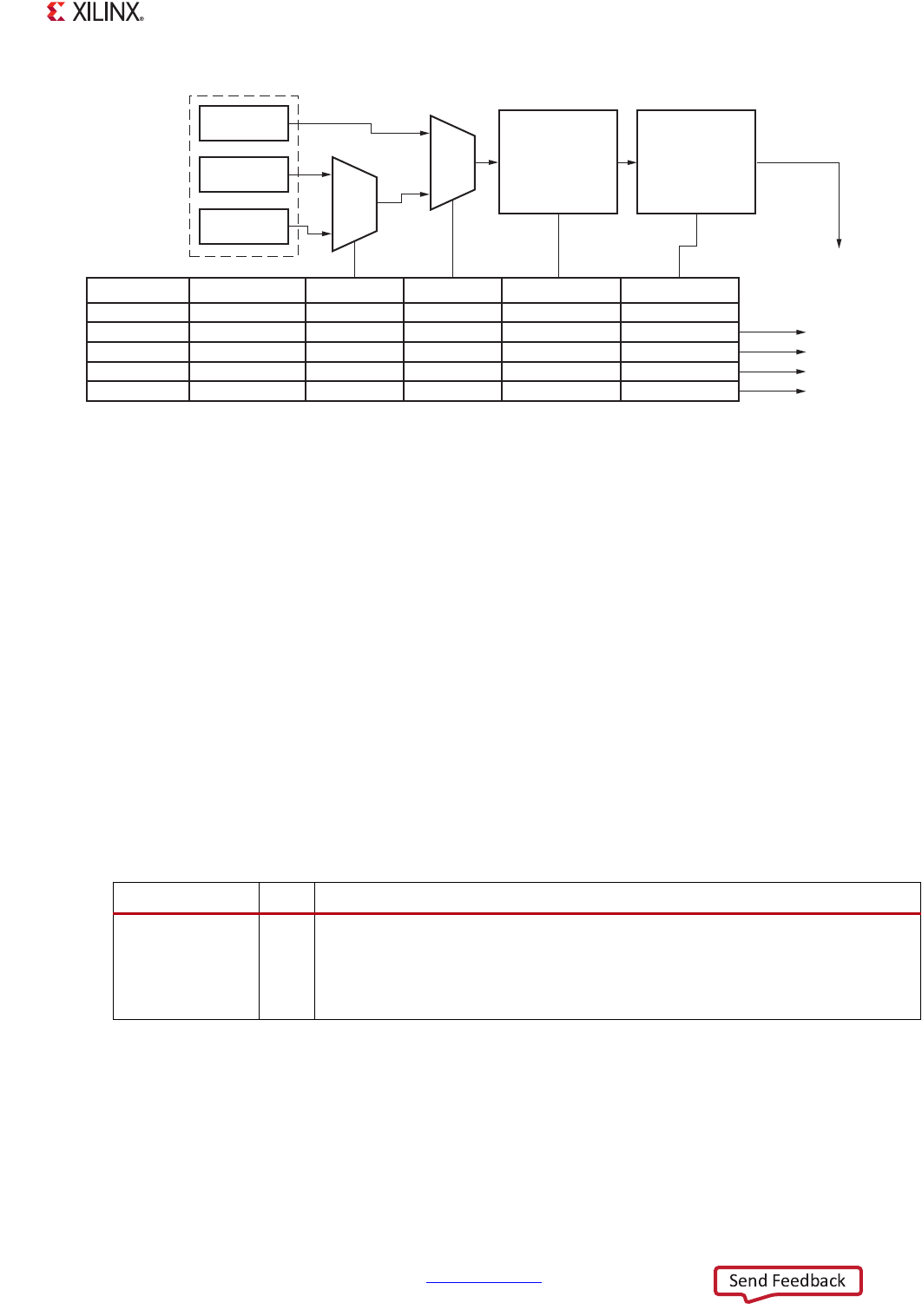
X-Ref Target - Figure 25-10
Figure 25-10: PL Clock Generation
UG585_c25_10_041612
IO PLL
ARM PLL
DDR PLL
Four
Independent
PL Clocks
6-bit
Programmable
Divisor 0
Glitch-Free
Divider 0 Ctrl FieldMux Ctrl FieldMux Ctrl FieldControl RegisterPL FCLK Clock Divider 1 Ctrl Field
PL FCLK 0
DIVISOR 0, 13:8SRCSEL, 5SRCSEL, 4FPGA0_CLK_CTRL
DIVISOR 1, 25:20
Glitch-
Free
0
1
6-bit
Programmable
Divisor 1
Glitch-Free
FCLKCLK0
PL FCLK 1
DIVISOR 0, 13:8SRCSEL, 5SRCSEL, 4FPGA1_CLK_CTRL
DIVISOR 1, 25:20
FCLKCLK1
PL FCLK 2
DIVISOR 0, 13:8SRCSEL, 5SRCSEL, 4FPGA2_CLK_CTRL
DIVISOR 1, 25:20
FCLKCLK2
PL FCLK 3
DIVISOR 0, 13:8SRCSEL, 5SRCSEL, 4FPGA3_CLK_CTRL
DIVISOR 1, 25:20
FCLKCLK3
Glitch-
Free
0
1
Table 25-4: PL Clock Throttle Input Signal
Signal Name I/O Description
FCLKCLKTRIGxN I The PL clock trigger signal is an input from the PL logic and is used to halt (pause)
the PL clock when counting a programmed number of clock pulses. The halt mode
is entered by the rising edge (logic 0 to logic 1) of the FCLKCLKTRIGxN signal. This
signal can be asserted asynchronously to the FCLK and all other signals. This pin
has no affect when the clock is running continuously, [LAST_CNT] = 0.