
User manual


Table Of Contents
- Zynq-7000 All Programmable SoC
- Table of Contents
- Ch. 1: Introduction
- Ch. 2: Signals, Interfaces, and Pins
- Ch. 3: Application Processing Unit
- Ch. 4: System Addresses
- Ch. 5: Interconnect
- Ch. 6: Boot and Configuration
- Ch. 7: Interrupts
- Ch. 8: Timers
- Ch. 9: DMA Controller
- Introduction
- Functional Description
- DMA Transfers on the AXI Interconnect
- AXI Transaction Considerations
- DMA Manager
- Multi-channel Data FIFO (MFIFO)
- Memory-to-Memory Transfers
- PL Peripheral AXI Transactions
- PL Peripheral Request Interface
- PL Peripheral - Length Managed by PL Peripheral
- PL Peripheral - Length Managed by DMAC
- Events and Interrupts
- Aborts
- Security
- IP Configuration Options
- Programming Guide for DMA Controller
- Programming Guide for DMA Engine
- Programming Restrictions
- System Functions
- I/O Interface
- Ch. 10: DDR Memory Controller
- Introduction
- AXI Memory Port Interface (DDRI)
- DDR Core and Transaction Scheduler (DDRC)
- DDRC Arbitration
- Controller PHY (DDRP)
- Initialization and Calibration
- DDR Clock Initialization
- DDR IOB Impedance Calibration
- DDR IOB Configuration
- DDR Controller Register Programming
- DRAM Reset and Initialization
- DRAM Input Impedance (ODT) Calibration
- DRAM Output Impedance (RON) Calibration
- DRAM Training
- Write Data Eye Adjustment
- Alternatives to Automatic DRAM Training
- DRAM Write Latency Restriction
- Register Overview
- Error Correction Code (ECC)
- Programming Model
- Ch. 11: Static Memory Controller
- Ch. 12: Quad-SPI Flash Controller
- Ch. 13: SD/SDIO Controller
- Ch. 14: General Purpose I/O (GPIO)
- Ch. 15: USB Host, Device, and OTG Controller
- Introduction
- Functional Description
- Programming Overview and Reference
- Device Mode Control
- Device Endpoint Data Structures
- Device Endpoint Packet Operational Model
- Device Endpoint Descriptor Reference
- Programming Guide for Device Controller
- Programming Guide for Device Endpoint Data Structures
- Host Mode Data Structures
- EHCI Implementation
- Host Data Structures Reference
- Programming Guide for Host Controller
- OTG Description and Reference
- System Functions
- I/O Interfaces
- Ch. 16: Gigabit Ethernet Controller
- Ch. 17: SPI Controller
- Ch. 18: CAN Controller
- Ch. 19: UART Controller
- Ch. 20: I2C Controller
- Ch. 21: Programmable Logic Description
- Ch. 22: Programmable Logic Design Guide
- Ch. 23: Programmable Logic Test and Debug
- Ch. 24: Power Management
- Ch. 25: Clocks
- Ch. 26: Reset System
- Ch. 27: JTAG and DAP Subsystem
- Ch. 28: System Test and Debug
- Ch. 29: On-Chip Memory (OCM)
- Ch. 30: XADC Interface
- Ch. 31: PCI Express
- Ch. 32: Device Secure Boot
- Appx. A: Additional Resources
- Appx. B: Register Details
- Overview
- Acronyms
- Module Summary
- AXI_HP Interface (AFI) (axi_hp)
- CAN Controller (can)
- DDR Memory Controller (ddrc)
- CoreSight Cross Trigger Interface (cti)
- Performance Monitor Unit (cortexa9_pmu)
- CoreSight Program Trace Macrocell (ptm)
- Debug Access Port (dap)
- CoreSight Embedded Trace Buffer (etb)
- PL Fabric Trace Monitor (ftm)
- CoreSight Trace Funnel (funnel)
- CoreSight Intstrumentation Trace Macrocell (itm)
- CoreSight Trace Packet Output (tpiu)
- Device Configuration Interface (devcfg)
- DMA Controller (dmac)
- Gigabit Ethernet Controller (GEM)
- General Purpose I/O (gpio)
- Interconnect QoS (qos301)
- NIC301 Address Region Control (nic301_addr_region_ctrl_registers)
- I2C Controller (IIC)
- L2 Cache (L2Cpl310)
- Application Processing Unit (mpcore)
- On-Chip Memory (ocm)
- Quad-SPI Flash Controller (qspi)
- SD Controller (sdio)
- System Level Control Registers (slcr)
- Static Memory Controller (pl353)
- SPI Controller (SPI)
- System Watchdog Timer (swdt)
- Triple Timer Counter (ttc)
- UART Controller (UART)
- USB Controller (usb)
Zynq-7000 AP SoC Technical Reference Manual www.xilinx.com 698
UG585 (v1.11) September 27, 2016
Chapter 25: Clocks
2. Force the PLL into bypass mode by writing a 1 to ARM_PLL_CTRL [PLL_BYPASS_FORCE, 4] and
setting the ARM_PLL_CTRL [PLL_BYPASS_QUAL, 3] bit to a 0. This de-asserts the reset to the ARM
PLL.
3. Assert and de-assert the PLL reset by writing a 1 and then a 0 to ARM_PLL_CTRL [PLL_RESET, 0].
4. Verify that the PLL is locked by reading PLL_STATUS [ARM_PLL_LOCK, 3].
5. Disable the PLL bypass mode by writing a 0 to ARM_PLL_CTRL [4].
The DDR and I/O PLLs are programmed in a similar fashion.
Software-Controlled PLL Update
The following steps are required for software to update the PLL clock frequency. This example is for
the I/O PLL. Table 25-6 shows the possible multiplier values and the required settings for each of
those multiplier values.
1. Program the IO_PLL_CTRL[PLL_FDIV] value and the PLL configuration register, IO_PLL_CFG
[LOCK_CNT, PLL_CP, PLL_RES].
2. Force the PLL into bypass mode by writing a 1 to IO_PLL_CTRL [PLL_BYPASS_FORCE, 4]. (When the
PLL goes into reset in the next step, its output will be undefined.)
3. Assert and de-assert the PLL reset by writing 1 and then a 0 to IO_PLL_CTRL [PLL_RESET, 0]. (This
is when the new values from step one are actually consumed by the PLL.)
4. Verify that the PLL is locked by reading PLL_STATUS [IO_PLL_LOCK, 2].
5. Disable the PLL bypass mode by writing a 0 to IO_PLL_CTRL [4].
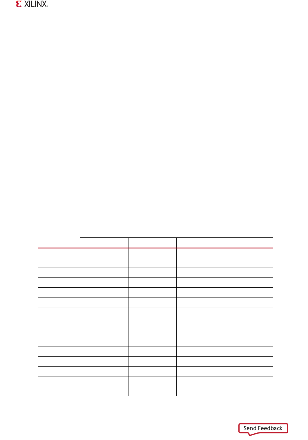
Table 25-6: PLL Frequency Control Settings
Desired PLL
Multiplier
Required PLL Control and Configuration Bit Fields
PLL_FDIV PLL CP PLL RES LOCK CNT
13 13 2 6 750
14 14 2 6 700
15 15 2 6 650
16 16 2 10 625
17 17 2 10 575
18 18 2 10 550
19 19 2 10 525
20 20 2 12 500
21 21 2 12 475
22 22 2 12 450
23 23 2 12 425
24 ~ 25 24 ~ 25 2 12 400
26 26 2 12 375
27 ~ 28 27 ~ 28 2 12 350
29 ~ 30 29 ~ 30 2 12 325