
User manual


Table Of Contents
- Zynq-7000 All Programmable SoC
- Table of Contents
- Ch. 1: Introduction
- Ch. 2: Signals, Interfaces, and Pins
- Ch. 3: Application Processing Unit
- Ch. 4: System Addresses
- Ch. 5: Interconnect
- Ch. 6: Boot and Configuration
- Ch. 7: Interrupts
- Ch. 8: Timers
- Ch. 9: DMA Controller
- Introduction
- Functional Description
- DMA Transfers on the AXI Interconnect
- AXI Transaction Considerations
- DMA Manager
- Multi-channel Data FIFO (MFIFO)
- Memory-to-Memory Transfers
- PL Peripheral AXI Transactions
- PL Peripheral Request Interface
- PL Peripheral - Length Managed by PL Peripheral
- PL Peripheral - Length Managed by DMAC
- Events and Interrupts
- Aborts
- Security
- IP Configuration Options
- Programming Guide for DMA Controller
- Programming Guide for DMA Engine
- Programming Restrictions
- System Functions
- I/O Interface
- Ch. 10: DDR Memory Controller
- Introduction
- AXI Memory Port Interface (DDRI)
- DDR Core and Transaction Scheduler (DDRC)
- DDRC Arbitration
- Controller PHY (DDRP)
- Initialization and Calibration
- DDR Clock Initialization
- DDR IOB Impedance Calibration
- DDR IOB Configuration
- DDR Controller Register Programming
- DRAM Reset and Initialization
- DRAM Input Impedance (ODT) Calibration
- DRAM Output Impedance (RON) Calibration
- DRAM Training
- Write Data Eye Adjustment
- Alternatives to Automatic DRAM Training
- DRAM Write Latency Restriction
- Register Overview
- Error Correction Code (ECC)
- Programming Model
- Ch. 11: Static Memory Controller
- Ch. 12: Quad-SPI Flash Controller
- Ch. 13: SD/SDIO Controller
- Ch. 14: General Purpose I/O (GPIO)
- Ch. 15: USB Host, Device, and OTG Controller
- Introduction
- Functional Description
- Programming Overview and Reference
- Device Mode Control
- Device Endpoint Data Structures
- Device Endpoint Packet Operational Model
- Device Endpoint Descriptor Reference
- Programming Guide for Device Controller
- Programming Guide for Device Endpoint Data Structures
- Host Mode Data Structures
- EHCI Implementation
- Host Data Structures Reference
- Programming Guide for Host Controller
- OTG Description and Reference
- System Functions
- I/O Interfaces
- Ch. 16: Gigabit Ethernet Controller
- Ch. 17: SPI Controller
- Ch. 18: CAN Controller
- Ch. 19: UART Controller
- Ch. 20: I2C Controller
- Ch. 21: Programmable Logic Description
- Ch. 22: Programmable Logic Design Guide
- Ch. 23: Programmable Logic Test and Debug
- Ch. 24: Power Management
- Ch. 25: Clocks
- Ch. 26: Reset System
- Ch. 27: JTAG and DAP Subsystem
- Ch. 28: System Test and Debug
- Ch. 29: On-Chip Memory (OCM)
- Ch. 30: XADC Interface
- Ch. 31: PCI Express
- Ch. 32: Device Secure Boot
- Appx. A: Additional Resources
- Appx. B: Register Details
- Overview
- Acronyms
- Module Summary
- AXI_HP Interface (AFI) (axi_hp)
- CAN Controller (can)
- DDR Memory Controller (ddrc)
- CoreSight Cross Trigger Interface (cti)
- Performance Monitor Unit (cortexa9_pmu)
- CoreSight Program Trace Macrocell (ptm)
- Debug Access Port (dap)
- CoreSight Embedded Trace Buffer (etb)
- PL Fabric Trace Monitor (ftm)
- CoreSight Trace Funnel (funnel)
- CoreSight Intstrumentation Trace Macrocell (itm)
- CoreSight Trace Packet Output (tpiu)
- Device Configuration Interface (devcfg)
- DMA Controller (dmac)
- Gigabit Ethernet Controller (GEM)
- General Purpose I/O (gpio)
- Interconnect QoS (qos301)
- NIC301 Address Region Control (nic301_addr_region_ctrl_registers)
- I2C Controller (IIC)
- L2 Cache (L2Cpl310)
- Application Processing Unit (mpcore)
- On-Chip Memory (ocm)
- Quad-SPI Flash Controller (qspi)
- SD Controller (sdio)
- System Level Control Registers (slcr)
- Static Memory Controller (pl353)
- SPI Controller (SPI)
- System Watchdog Timer (swdt)
- Triple Timer Counter (ttc)
- UART Controller (UART)
- USB Controller (usb)
Zynq-7000 AP SoC Technical Reference Manual www.xilinx.com 705
UG585 (v1.11) September 27, 2016
Chapter 26: Reset System
Debug system reset is a command from the ARM DAP which is controlled by JTAG. This causes the
system to reset, just like the external system reset.
Debug reset resets certain portions of the SoC debug block including the JTAG logic.
The PS does not support the external TRST, although it does support assertion of a reset sequence
using TMS. The JTAG logic is only reset at power-on reset or assertion of CDBGRSTREQ from the ARM
debug access port (DAP) Controller (JTAG). All of the logic in the JTAG TCK clock domain is reset by
this signal.
26.3 Reset Effects
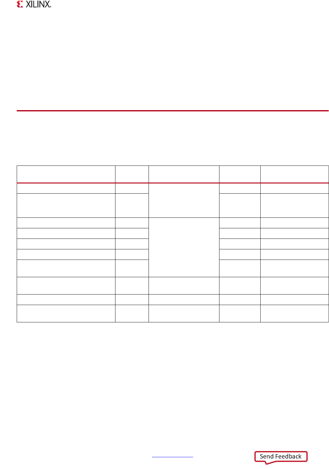
The effects of various resets are described in Table 26-1.
26.3.1 Peripherals
All PS peripherals are reset when the PS is reset. In addition, individual peripheral resets might also
be asserted under software control, through programmable bits within the SLCR.
Most peripherals have the ability to reset each of the clock domains within that peripheral. For
instance, the Ethernet controller can reset the RX side, TX side, or the interconnect side. Each clock
domain can be reset separately. Individual peripherals might have their own resets defined within
those blocks.
Peripheral resets do not result in the RAM memory clear logic being activated to clear all memories
within the design.
Table 26-1: Reset Effects
Reset Name Source
Portion of System that is
Reset
RAMs Cleared
slcr.REBOOT_STATUS
Bits set = 1
Power-On Reset (PS_POR_B) Device pin
Entire chip, including
debug (All)
The PL must be
re-programmed.
All [POR]
Security Lock Down
(requires a power-on reset to
recover)
DevC All N/A
External System Reset (PS_SRST_B) Device pin
All except debug and
persistent registers.
The PL must be
re-programmed.
All [SRST_RST]
System Software SLCR All [SLC_RST]
System Debug Reset JTAG All [DBG_RST]
System Watchdog Timer SWDT All [SWDT_RST]
CPU0 and CPU1 Watchdog Timers
(when slcr.RS_AWDT_CTRL{1,0} = 0)
AWDT All [AWDT{1,0}_RST]
CPU0 and CPU1 Watchdog Timers
(when slcr.RS_AWDT_CTRL{1,0} = 1)
AWDT CPU (s) only. None N/A
Debug Reset JTAG Debug logic. None N/A
Peripherals
SLCR
Selected peripherals or
CPUs.
None N/A