
User manual


Table Of Contents
- Zynq-7000 All Programmable SoC
- Table of Contents
- Ch. 1: Introduction
- Ch. 2: Signals, Interfaces, and Pins
- Ch. 3: Application Processing Unit
- Ch. 4: System Addresses
- Ch. 5: Interconnect
- Ch. 6: Boot and Configuration
- Ch. 7: Interrupts
- Ch. 8: Timers
- Ch. 9: DMA Controller
- Introduction
- Functional Description
- DMA Transfers on the AXI Interconnect
- AXI Transaction Considerations
- DMA Manager
- Multi-channel Data FIFO (MFIFO)
- Memory-to-Memory Transfers
- PL Peripheral AXI Transactions
- PL Peripheral Request Interface
- PL Peripheral - Length Managed by PL Peripheral
- PL Peripheral - Length Managed by DMAC
- Events and Interrupts
- Aborts
- Security
- IP Configuration Options
- Programming Guide for DMA Controller
- Programming Guide for DMA Engine
- Programming Restrictions
- System Functions
- I/O Interface
- Ch. 10: DDR Memory Controller
- Introduction
- AXI Memory Port Interface (DDRI)
- DDR Core and Transaction Scheduler (DDRC)
- DDRC Arbitration
- Controller PHY (DDRP)
- Initialization and Calibration
- DDR Clock Initialization
- DDR IOB Impedance Calibration
- DDR IOB Configuration
- DDR Controller Register Programming
- DRAM Reset and Initialization
- DRAM Input Impedance (ODT) Calibration
- DRAM Output Impedance (RON) Calibration
- DRAM Training
- Write Data Eye Adjustment
- Alternatives to Automatic DRAM Training
- DRAM Write Latency Restriction
- Register Overview
- Error Correction Code (ECC)
- Programming Model
- Ch. 11: Static Memory Controller
- Ch. 12: Quad-SPI Flash Controller
- Ch. 13: SD/SDIO Controller
- Ch. 14: General Purpose I/O (GPIO)
- Ch. 15: USB Host, Device, and OTG Controller
- Introduction
- Functional Description
- Programming Overview and Reference
- Device Mode Control
- Device Endpoint Data Structures
- Device Endpoint Packet Operational Model
- Device Endpoint Descriptor Reference
- Programming Guide for Device Controller
- Programming Guide for Device Endpoint Data Structures
- Host Mode Data Structures
- EHCI Implementation
- Host Data Structures Reference
- Programming Guide for Host Controller
- OTG Description and Reference
- System Functions
- I/O Interfaces
- Ch. 16: Gigabit Ethernet Controller
- Ch. 17: SPI Controller
- Ch. 18: CAN Controller
- Ch. 19: UART Controller
- Ch. 20: I2C Controller
- Ch. 21: Programmable Logic Description
- Ch. 22: Programmable Logic Design Guide
- Ch. 23: Programmable Logic Test and Debug
- Ch. 24: Power Management
- Ch. 25: Clocks
- Ch. 26: Reset System
- Ch. 27: JTAG and DAP Subsystem
- Ch. 28: System Test and Debug
- Ch. 29: On-Chip Memory (OCM)
- Ch. 30: XADC Interface
- Ch. 31: PCI Express
- Ch. 32: Device Secure Boot
- Appx. A: Additional Resources
- Appx. B: Register Details
- Overview
- Acronyms
- Module Summary
- AXI_HP Interface (AFI) (axi_hp)
- CAN Controller (can)
- DDR Memory Controller (ddrc)
- CoreSight Cross Trigger Interface (cti)
- Performance Monitor Unit (cortexa9_pmu)
- CoreSight Program Trace Macrocell (ptm)
- Debug Access Port (dap)
- CoreSight Embedded Trace Buffer (etb)
- PL Fabric Trace Monitor (ftm)
- CoreSight Trace Funnel (funnel)
- CoreSight Intstrumentation Trace Macrocell (itm)
- CoreSight Trace Packet Output (tpiu)
- Device Configuration Interface (devcfg)
- DMA Controller (dmac)
- Gigabit Ethernet Controller (GEM)
- General Purpose I/O (gpio)
- Interconnect QoS (qos301)
- NIC301 Address Region Control (nic301_addr_region_ctrl_registers)
- I2C Controller (IIC)
- L2 Cache (L2Cpl310)
- Application Processing Unit (mpcore)
- On-Chip Memory (ocm)
- Quad-SPI Flash Controller (qspi)
- SD Controller (sdio)
- System Level Control Registers (slcr)
- Static Memory Controller (pl353)
- SPI Controller (SPI)
- System Watchdog Timer (swdt)
- Triple Timer Counter (ttc)
- UART Controller (UART)
- USB Controller (usb)
Zynq-7000 AP SoC Technical Reference Manual www.xilinx.com 738
UG585 (v1.11) September 27, 2016
Chapter 29: On-Chip Memory (OCM)
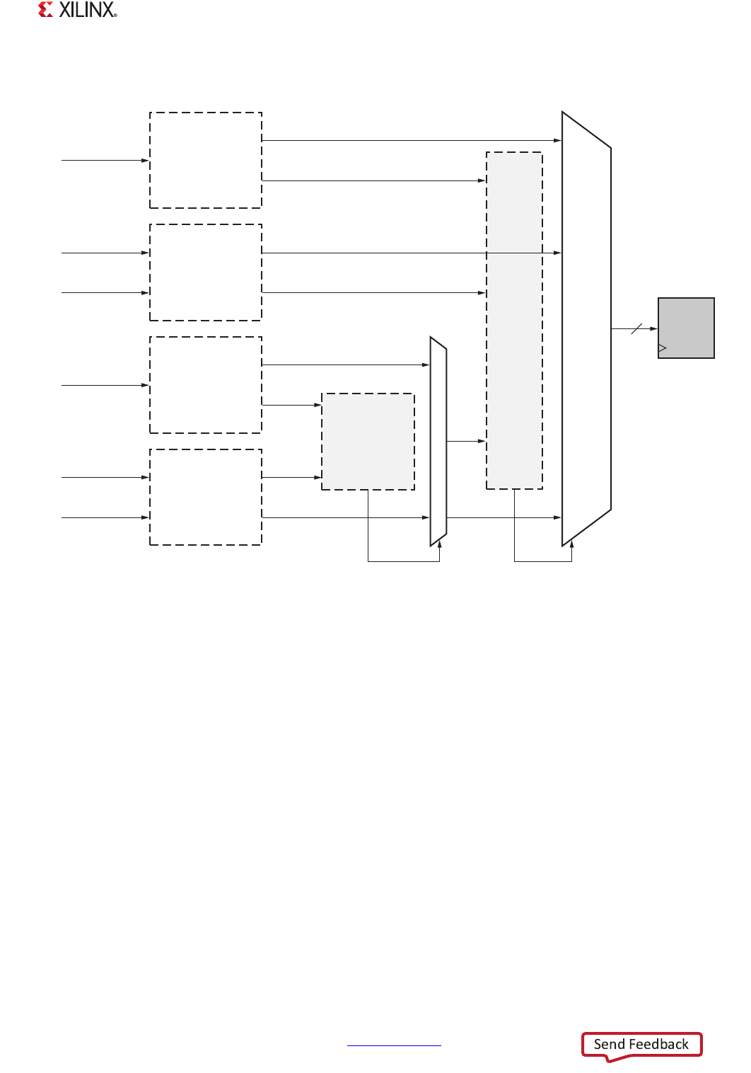
Arbitration is implemented as shown in Figure 29-3.
There is an additional round-robin pre-arbitration process that selects between a read or write
transaction on a per data-beat basis for the OCM-switch port traffic.
Note: Arbitration is performed on a transfer (data beat or clock cycle) basis, not on an AXI command
basis. The in-coming AXI read and write commands are split into individual addresses (or 128-bit
address pairs for aligned bursts) before arbitration.
Note: Each individual write address beat will not request access to the memory array until the write
data associated with it is available inside the OCM module — this prevents the scenario of a write
request being stalled due to write data not being available.
Starvation Scenarios
System constraints on the OCM are:
• The RAM array and OCM Switch port are clocked with CPU_2x which runs at one third or one
half the CPU clock.
• The SCU (CPU/ACP) port is clocked at full the CPU clock rate.
• Each of the four incoming AXI data channels are 64-bits wide.
X-Ref Target - Figure 29-3
Figure 29-3: Default (ScuWrPriorityLo=0) OCM Arbitration
UG585_c29_03_042512
Break Burst
Into Individual
Addresses Or
Address Pairs
(128-bit aligned)
256 KB
RAM
SCU
AXI64 RdCmd
Addr/Cmd
Req
Addr/Cmd/Data
Req
Addr/Cmd
Req
Req
Addr/Cmd/Data
Gnt[1:0]
Break Burst
Into Individual
Addresses Or
Address Pairs
(128-bit aligned)
SCU
AXI64 WrCmd
SCU
AXI64 WrData
Break Burst
Into Individual
Addresses Or
Address Pairs
(128-bit aligned)
OCM Switch
AXI64 RdCmd
Gnt[2:0]
Req
Hi
Priority
Med
Priority
Low
Priority
OCM
Switch
RoundRobin
Arbiter
Fixed
Priority
Arbiter
Break Burst
Into Individual
Addresses Or
Address Pairs
(128-bit aligned)
OCM Switch
AXI64 WrCmd
OCM Switch
AXI64 WrData
128