
User manual


Table Of Contents
- Zynq-7000 All Programmable SoC
- Table of Contents
- Ch. 1: Introduction
- Ch. 2: Signals, Interfaces, and Pins
- Ch. 3: Application Processing Unit
- Ch. 4: System Addresses
- Ch. 5: Interconnect
- Ch. 6: Boot and Configuration
- Ch. 7: Interrupts
- Ch. 8: Timers
- Ch. 9: DMA Controller
- Introduction
- Functional Description
- DMA Transfers on the AXI Interconnect
- AXI Transaction Considerations
- DMA Manager
- Multi-channel Data FIFO (MFIFO)
- Memory-to-Memory Transfers
- PL Peripheral AXI Transactions
- PL Peripheral Request Interface
- PL Peripheral - Length Managed by PL Peripheral
- PL Peripheral - Length Managed by DMAC
- Events and Interrupts
- Aborts
- Security
- IP Configuration Options
- Programming Guide for DMA Controller
- Programming Guide for DMA Engine
- Programming Restrictions
- System Functions
- I/O Interface
- Ch. 10: DDR Memory Controller
- Introduction
- AXI Memory Port Interface (DDRI)
- DDR Core and Transaction Scheduler (DDRC)
- DDRC Arbitration
- Controller PHY (DDRP)
- Initialization and Calibration
- DDR Clock Initialization
- DDR IOB Impedance Calibration
- DDR IOB Configuration
- DDR Controller Register Programming
- DRAM Reset and Initialization
- DRAM Input Impedance (ODT) Calibration
- DRAM Output Impedance (RON) Calibration
- DRAM Training
- Write Data Eye Adjustment
- Alternatives to Automatic DRAM Training
- DRAM Write Latency Restriction
- Register Overview
- Error Correction Code (ECC)
- Programming Model
- Ch. 11: Static Memory Controller
- Ch. 12: Quad-SPI Flash Controller
- Ch. 13: SD/SDIO Controller
- Ch. 14: General Purpose I/O (GPIO)
- Ch. 15: USB Host, Device, and OTG Controller
- Introduction
- Functional Description
- Programming Overview and Reference
- Device Mode Control
- Device Endpoint Data Structures
- Device Endpoint Packet Operational Model
- Device Endpoint Descriptor Reference
- Programming Guide for Device Controller
- Programming Guide for Device Endpoint Data Structures
- Host Mode Data Structures
- EHCI Implementation
- Host Data Structures Reference
- Programming Guide for Host Controller
- OTG Description and Reference
- System Functions
- I/O Interfaces
- Ch. 16: Gigabit Ethernet Controller
- Ch. 17: SPI Controller
- Ch. 18: CAN Controller
- Ch. 19: UART Controller
- Ch. 20: I2C Controller
- Ch. 21: Programmable Logic Description
- Ch. 22: Programmable Logic Design Guide
- Ch. 23: Programmable Logic Test and Debug
- Ch. 24: Power Management
- Ch. 25: Clocks
- Ch. 26: Reset System
- Ch. 27: JTAG and DAP Subsystem
- Ch. 28: System Test and Debug
- Ch. 29: On-Chip Memory (OCM)
- Ch. 30: XADC Interface
- Ch. 31: PCI Express
- Ch. 32: Device Secure Boot
- Appx. A: Additional Resources
- Appx. B: Register Details
- Overview
- Acronyms
- Module Summary
- AXI_HP Interface (AFI) (axi_hp)
- CAN Controller (can)
- DDR Memory Controller (ddrc)
- CoreSight Cross Trigger Interface (cti)
- Performance Monitor Unit (cortexa9_pmu)
- CoreSight Program Trace Macrocell (ptm)
- Debug Access Port (dap)
- CoreSight Embedded Trace Buffer (etb)
- PL Fabric Trace Monitor (ftm)
- CoreSight Trace Funnel (funnel)
- CoreSight Intstrumentation Trace Macrocell (itm)
- CoreSight Trace Packet Output (tpiu)
- Device Configuration Interface (devcfg)
- DMA Controller (dmac)
- Gigabit Ethernet Controller (GEM)
- General Purpose I/O (gpio)
- Interconnect QoS (qos301)
- NIC301 Address Region Control (nic301_addr_region_ctrl_registers)
- I2C Controller (IIC)
- L2 Cache (L2Cpl310)
- Application Processing Unit (mpcore)
- On-Chip Memory (ocm)
- Quad-SPI Flash Controller (qspi)
- SD Controller (sdio)
- System Level Control Registers (slcr)
- Static Memory Controller (pl353)
- SPI Controller (SPI)
- System Watchdog Timer (swdt)
- Triple Timer Counter (ttc)
- UART Controller (UART)
- USB Controller (usb)
Zynq-7000 AP SoC Technical Reference Manual www.xilinx.com 740
UG585 (v1.11) September 27, 2016
Chapter 29: On-Chip Memory (OCM)
• All other masters that do not pass through the SCU are always unable to access the lower
512 KB of DDR in the OCM's low address range (0x0000_0000 to 0x0007_FFFF).
• Accesses to addresses which the RAM array is not currently mapped to are given an error
response.
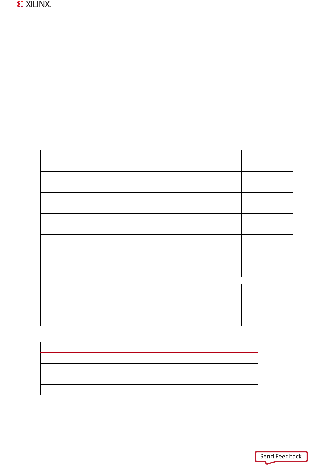
Initial View
Upon entering user mode, the BootROM is no longer accessible, and the RAM space is split. Note
that one 64 KB range resides at the high OCM address, and the other 192 KB resides at the lower
address range. Table 29-1 and Table 29-2 identify the initial OCM/DDR address map and register
settings, respectively.
Attempted accesses to reserved areas return all zeroes along with a SLVERR bus response.
Table 29-1: Initial OCM/DDR Address Map
Address Range (Hex) Size CPUs/ACP Other Masters
0000_0000 - 0000_FFFF 64 KB OCM OCM
0001_0000 - 0001_FFFF 64 KB OCM OCM
0002_0000 - 0002_FFFF 64 KB OCM OCM
0003_0000 - 0003_FFFF 64 KB Reserved Reserved
0004_0000 - 0007_FFFF 256 KB Reserved Reserved
0008_0000 - 000B_FFFF 256 KB Reserved DDR
000C_0000 - 000C_FFFF 64 KB Reserved DDR
000D_0000 - 000D_FFFF 64 KB Reserved DDR
000E_0000 - 000E_FFFF 64 KB Reserved DDR
000F_0000 - 000F_FFFF 64 KB OCM3 (alias) DDR
0010_0000 - 3FFF_FFFF 1,023 MB DDR DDR
FFFC_0000 - FFFC_FFFF 64 KB Reserved Reserved
FFFD_0000 - FFFD_FFFF 64 KB Reserved Reserved
FFFE_0000 - FFFE_FFFF 64 KB Reserved Reserved
FFFF_0000 - FFFF_FFFF 64 KB OCM3 OCM3
Table 29-2: Initial Register Settings
Register Value
slcr.OCM_CFG[RAM_HI] 1000
mpcore.SCU_CONTROL_REGISTER[Address_filtering_enable] 1
mpcore.Filtering_Start_Address_Register 0x0010_0000
mpcore.Filtering_End_Address_Register 0xFFE0_0000