
User manual


Table Of Contents
- Zynq-7000 All Programmable SoC
- Table of Contents
- Ch. 1: Introduction
- Ch. 2: Signals, Interfaces, and Pins
- Ch. 3: Application Processing Unit
- Ch. 4: System Addresses
- Ch. 5: Interconnect
- Ch. 6: Boot and Configuration
- Ch. 7: Interrupts
- Ch. 8: Timers
- Ch. 9: DMA Controller
- Introduction
- Functional Description
- DMA Transfers on the AXI Interconnect
- AXI Transaction Considerations
- DMA Manager
- Multi-channel Data FIFO (MFIFO)
- Memory-to-Memory Transfers
- PL Peripheral AXI Transactions
- PL Peripheral Request Interface
- PL Peripheral - Length Managed by PL Peripheral
- PL Peripheral - Length Managed by DMAC
- Events and Interrupts
- Aborts
- Security
- IP Configuration Options
- Programming Guide for DMA Controller
- Programming Guide for DMA Engine
- Programming Restrictions
- System Functions
- I/O Interface
- Ch. 10: DDR Memory Controller
- Introduction
- AXI Memory Port Interface (DDRI)
- DDR Core and Transaction Scheduler (DDRC)
- DDRC Arbitration
- Controller PHY (DDRP)
- Initialization and Calibration
- DDR Clock Initialization
- DDR IOB Impedance Calibration
- DDR IOB Configuration
- DDR Controller Register Programming
- DRAM Reset and Initialization
- DRAM Input Impedance (ODT) Calibration
- DRAM Output Impedance (RON) Calibration
- DRAM Training
- Write Data Eye Adjustment
- Alternatives to Automatic DRAM Training
- DRAM Write Latency Restriction
- Register Overview
- Error Correction Code (ECC)
- Programming Model
- Ch. 11: Static Memory Controller
- Ch. 12: Quad-SPI Flash Controller
- Ch. 13: SD/SDIO Controller
- Ch. 14: General Purpose I/O (GPIO)
- Ch. 15: USB Host, Device, and OTG Controller
- Introduction
- Functional Description
- Programming Overview and Reference
- Device Mode Control
- Device Endpoint Data Structures
- Device Endpoint Packet Operational Model
- Device Endpoint Descriptor Reference
- Programming Guide for Device Controller
- Programming Guide for Device Endpoint Data Structures
- Host Mode Data Structures
- EHCI Implementation
- Host Data Structures Reference
- Programming Guide for Host Controller
- OTG Description and Reference
- System Functions
- I/O Interfaces
- Ch. 16: Gigabit Ethernet Controller
- Ch. 17: SPI Controller
- Ch. 18: CAN Controller
- Ch. 19: UART Controller
- Ch. 20: I2C Controller
- Ch. 21: Programmable Logic Description
- Ch. 22: Programmable Logic Design Guide
- Ch. 23: Programmable Logic Test and Debug
- Ch. 24: Power Management
- Ch. 25: Clocks
- Ch. 26: Reset System
- Ch. 27: JTAG and DAP Subsystem
- Ch. 28: System Test and Debug
- Ch. 29: On-Chip Memory (OCM)
- Ch. 30: XADC Interface
- Ch. 31: PCI Express
- Ch. 32: Device Secure Boot
- Appx. A: Additional Resources
- Appx. B: Register Details
- Overview
- Acronyms
- Module Summary
- AXI_HP Interface (AFI) (axi_hp)
- CAN Controller (can)
- DDR Memory Controller (ddrc)
- CoreSight Cross Trigger Interface (cti)
- Performance Monitor Unit (cortexa9_pmu)
- CoreSight Program Trace Macrocell (ptm)
- Debug Access Port (dap)
- CoreSight Embedded Trace Buffer (etb)
- PL Fabric Trace Monitor (ftm)
- CoreSight Trace Funnel (funnel)
- CoreSight Intstrumentation Trace Macrocell (itm)
- CoreSight Trace Packet Output (tpiu)
- Device Configuration Interface (devcfg)
- DMA Controller (dmac)
- Gigabit Ethernet Controller (GEM)
- General Purpose I/O (gpio)
- Interconnect QoS (qos301)
- NIC301 Address Region Control (nic301_addr_region_ctrl_registers)
- I2C Controller (IIC)
- L2 Cache (L2Cpl310)
- Application Processing Unit (mpcore)
- On-Chip Memory (ocm)
- Quad-SPI Flash Controller (qspi)
- SD Controller (sdio)
- System Level Control Registers (slcr)
- Static Memory Controller (pl353)
- SPI Controller (SPI)
- System Watchdog Timer (swdt)
- Triple Timer Counter (ttc)
- UART Controller (UART)
- USB Controller (usb)
Zynq-7000 AP SoC Technical Reference Manual www.xilinx.com 742
UG585 (v1.11) September 27, 2016
Chapter 29: On-Chip Memory (OCM)
These other bus masters always see the OCM with accesses (from address 0x0000_0000 to
0x0007_FFFF and address 0xFFFC_0000 to 0xFFFF_FFFF) going to OCM space. Depending on
how the SLCR OCM registers are configured, these accesses either terminate at the RAM array or to
a default reserved address, resulting in an AXI SLVERR error. These other masters potentially see gaps
in the RAM address maps.
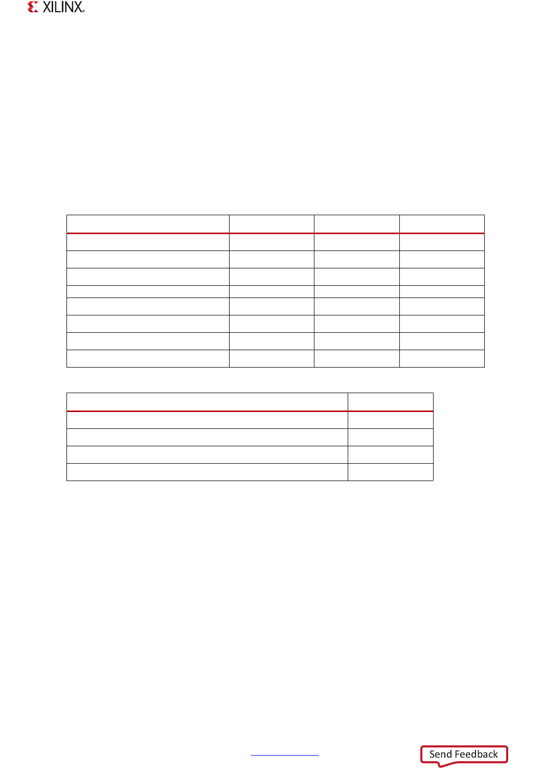
The CPU/ACP view, however, can be different using the SCU address filtering. For example, if the CPU
wants DDR DRAM to be located at address 0x0000_0000, it can configure the address filtering and
SLCR OCM registers so that the address map shown in Table 29-5 is seen. In Table 29-5, note that the
CPU/ACP masters are able to address the entire DDR address range, while all other masters cannot
address the lower 512 KB of DDR. Table 29-6 identifies example of OCM relocation register settings.
29.2.6 Interrupts
The OCM module is able to assert an interrupt signal to the APU under the following circumstances:
• Single-bit Parity Error
• Multiple-bit Parity Error
• Unsupported LOCK Request
All interrupts are enabled via the OCM.OCM_PARITY_CTRL register. Individual interrupt status is
accessed via the OCM.OCM_IRQ_STS register, and cleared with a write of 1 to each bit location.
Parity on the RAM array is performed when the OCM.OCM_PARITY_CTRL[ParityCheckDis] is not
asserted. When parity checking is enabled, a single- or multi-bit parity error sets the appropriate
interrupt status, and triggers an external interrupt if the associated enable bit is set. The address
offset of the first parity error is stored in the OCM.OCM_PARITY_ERRADDRESS register. For reads, a
Table 29-5: Example SCU Address Filtering Address Map
Address Range (Hex) Size CPUs/ACP Other Masters
0000_0000 - 0007_FFFF 512 KB DDR Reserved
0008_0000 - 000F_FFFF 512 KB DDR DDR
0010_0000 - 3FFF_FFFF 1,023 MB DDR DDR
FFFC_0000 - FFFC_FFFF 64 KB OCM0 OCM0
FFFD_0000 - FFFD_FFFF 64 KB OCM1 OCM1
FFFE_0000 - FFFE_FFFF 64 KB OCM2 OCM2
FFFF_0000 - FFFF_FFFF 64 KB OCM3 OCM3
Table 29-6: Example OCM Relocation Register Settings
Register Value
slcr.OCM_CFG[RAM_HI] 1111
mpcore.SCU_CONTROL_REGISTER[Address_filtering_enable] 1
mpcore.Filtering_Start_Address_Register 0x0000_0000
mpcore.Filtering_End_Address_Register 0xFFE0_0000