
User manual


Table Of Contents
- Zynq-7000 All Programmable SoC
- Table of Contents
- Ch. 1: Introduction
- Ch. 2: Signals, Interfaces, and Pins
- Ch. 3: Application Processing Unit
- Ch. 4: System Addresses
- Ch. 5: Interconnect
- Ch. 6: Boot and Configuration
- Ch. 7: Interrupts
- Ch. 8: Timers
- Ch. 9: DMA Controller
- Introduction
- Functional Description
- DMA Transfers on the AXI Interconnect
- AXI Transaction Considerations
- DMA Manager
- Multi-channel Data FIFO (MFIFO)
- Memory-to-Memory Transfers
- PL Peripheral AXI Transactions
- PL Peripheral Request Interface
- PL Peripheral - Length Managed by PL Peripheral
- PL Peripheral - Length Managed by DMAC
- Events and Interrupts
- Aborts
- Security
- IP Configuration Options
- Programming Guide for DMA Controller
- Programming Guide for DMA Engine
- Programming Restrictions
- System Functions
- I/O Interface
- Ch. 10: DDR Memory Controller
- Introduction
- AXI Memory Port Interface (DDRI)
- DDR Core and Transaction Scheduler (DDRC)
- DDRC Arbitration
- Controller PHY (DDRP)
- Initialization and Calibration
- DDR Clock Initialization
- DDR IOB Impedance Calibration
- DDR IOB Configuration
- DDR Controller Register Programming
- DRAM Reset and Initialization
- DRAM Input Impedance (ODT) Calibration
- DRAM Output Impedance (RON) Calibration
- DRAM Training
- Write Data Eye Adjustment
- Alternatives to Automatic DRAM Training
- DRAM Write Latency Restriction
- Register Overview
- Error Correction Code (ECC)
- Programming Model
- Ch. 11: Static Memory Controller
- Ch. 12: Quad-SPI Flash Controller
- Ch. 13: SD/SDIO Controller
- Ch. 14: General Purpose I/O (GPIO)
- Ch. 15: USB Host, Device, and OTG Controller
- Introduction
- Functional Description
- Programming Overview and Reference
- Device Mode Control
- Device Endpoint Data Structures
- Device Endpoint Packet Operational Model
- Device Endpoint Descriptor Reference
- Programming Guide for Device Controller
- Programming Guide for Device Endpoint Data Structures
- Host Mode Data Structures
- EHCI Implementation
- Host Data Structures Reference
- Programming Guide for Host Controller
- OTG Description and Reference
- System Functions
- I/O Interfaces
- Ch. 16: Gigabit Ethernet Controller
- Ch. 17: SPI Controller
- Ch. 18: CAN Controller
- Ch. 19: UART Controller
- Ch. 20: I2C Controller
- Ch. 21: Programmable Logic Description
- Ch. 22: Programmable Logic Design Guide
- Ch. 23: Programmable Logic Test and Debug
- Ch. 24: Power Management
- Ch. 25: Clocks
- Ch. 26: Reset System
- Ch. 27: JTAG and DAP Subsystem
- Ch. 28: System Test and Debug
- Ch. 29: On-Chip Memory (OCM)
- Ch. 30: XADC Interface
- Ch. 31: PCI Express
- Ch. 32: Device Secure Boot
- Appx. A: Additional Resources
- Appx. B: Register Details
- Overview
- Acronyms
- Module Summary
- AXI_HP Interface (AFI) (axi_hp)
- CAN Controller (can)
- DDR Memory Controller (ddrc)
- CoreSight Cross Trigger Interface (cti)
- Performance Monitor Unit (cortexa9_pmu)
- CoreSight Program Trace Macrocell (ptm)
- Debug Access Port (dap)
- CoreSight Embedded Trace Buffer (etb)
- PL Fabric Trace Monitor (ftm)
- CoreSight Trace Funnel (funnel)
- CoreSight Intstrumentation Trace Macrocell (itm)
- CoreSight Trace Packet Output (tpiu)
- Device Configuration Interface (devcfg)
- DMA Controller (dmac)
- Gigabit Ethernet Controller (GEM)
- General Purpose I/O (gpio)
- Interconnect QoS (qos301)
- NIC301 Address Region Control (nic301_addr_region_ctrl_registers)
- I2C Controller (IIC)
- L2 Cache (L2Cpl310)
- Application Processing Unit (mpcore)
- On-Chip Memory (ocm)
- Quad-SPI Flash Controller (qspi)
- SD Controller (sdio)
- System Level Control Registers (slcr)
- Static Memory Controller (pl353)
- SPI Controller (SPI)
- System Watchdog Timer (swdt)
- Triple Timer Counter (ttc)
- UART Controller (UART)
- USB Controller (usb)
Zynq-7000 AP SoC Technical Reference Manual www.xilinx.com 747
UG585 (v1.11) September 27, 2016
Chapter 30: XADC Interface
• Uses the JTAG TAP controller to access the XADC registers
• Enables JTAG access to all XADC registers including ADC measurements
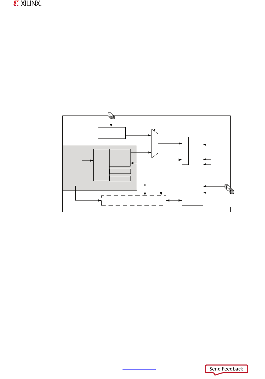
30.1.2 System Viewpoint
The XADC is a implemented in hard logic and resides in the PL power domain. The PS-XADC interface
is part of the PS and can be accessed by the PS APU without the PL being programmed. The PL must
be powered up to configure the PS-XADC interface, use the PL-JTAG or DRP interfaces, and to
operate the XADC. A system level block diagram is shown in Figure 30-1.
Note: The XADC arbitrates between the DRP interface and either the PS-XADC or the PL-JTAG
interface.
PS-XADC Interface
The PS-XADC interface description consumes the majority of this chapter. Software running in the PS
configures the interface using the devcfg registers. Software writes commands to the interface that
are pushed into the Command FIFO. These 32-bit writes, consisting of DRP command, address and
data, are serialized and sent to the XADC in a loopback path that fills the returning Read Data FIFO
that is read by the software.
The interface is configured by the devcfg registers, refer to Appendix B, Register Details.
DRP Interface
The DRP interface is a parallel 16-bit bidirectional interface that can connect to a PL bus master via
the LogiCORE IP AXI XADC PL logic using an AXI4-Lite interface to enable the PS or a MicroBlaze
X-Ref Target - Figure 30-1
Figure 30-1: XADC Module System Viewpoint
PS
PL
Zynq-7000 AP SoC Device
PS-XADC
Interrupt Status
32-bit APB
Slave
(from Master
Interconnect)
DevC
(devcfg)
Security
PCAP
XADC
Arbitor
Internal
Voltages
LogiCORE IP AXI XADC Core Logic
External
Voltages
PL-JTAG
Interface
32-bit AXI
(M_AXI_GP)
JTAG
Dedicated
pins in PL
devcfg.XADCIF_CFG [31]
0
1
Internal
Temperature
Serial
Alarm and OT
Signals
Refer to the PG019 Product Specification
Configured by
Bitstream or via
DRP commands.
DRP
Serial
Dual purpose
PL pins.
16-bit data
Misc.
Signals
UG585_c30_10_021913