
User manual


Table Of Contents
- Zynq-7000 All Programmable SoC
- Table of Contents
- Ch. 1: Introduction
- Ch. 2: Signals, Interfaces, and Pins
- Ch. 3: Application Processing Unit
- Ch. 4: System Addresses
- Ch. 5: Interconnect
- Ch. 6: Boot and Configuration
- Ch. 7: Interrupts
- Ch. 8: Timers
- Ch. 9: DMA Controller
- Introduction
- Functional Description
- DMA Transfers on the AXI Interconnect
- AXI Transaction Considerations
- DMA Manager
- Multi-channel Data FIFO (MFIFO)
- Memory-to-Memory Transfers
- PL Peripheral AXI Transactions
- PL Peripheral Request Interface
- PL Peripheral - Length Managed by PL Peripheral
- PL Peripheral - Length Managed by DMAC
- Events and Interrupts
- Aborts
- Security
- IP Configuration Options
- Programming Guide for DMA Controller
- Programming Guide for DMA Engine
- Programming Restrictions
- System Functions
- I/O Interface
- Ch. 10: DDR Memory Controller
- Introduction
- AXI Memory Port Interface (DDRI)
- DDR Core and Transaction Scheduler (DDRC)
- DDRC Arbitration
- Controller PHY (DDRP)
- Initialization and Calibration
- DDR Clock Initialization
- DDR IOB Impedance Calibration
- DDR IOB Configuration
- DDR Controller Register Programming
- DRAM Reset and Initialization
- DRAM Input Impedance (ODT) Calibration
- DRAM Output Impedance (RON) Calibration
- DRAM Training
- Write Data Eye Adjustment
- Alternatives to Automatic DRAM Training
- DRAM Write Latency Restriction
- Register Overview
- Error Correction Code (ECC)
- Programming Model
- Ch. 11: Static Memory Controller
- Ch. 12: Quad-SPI Flash Controller
- Ch. 13: SD/SDIO Controller
- Ch. 14: General Purpose I/O (GPIO)
- Ch. 15: USB Host, Device, and OTG Controller
- Introduction
- Functional Description
- Programming Overview and Reference
- Device Mode Control
- Device Endpoint Data Structures
- Device Endpoint Packet Operational Model
- Device Endpoint Descriptor Reference
- Programming Guide for Device Controller
- Programming Guide for Device Endpoint Data Structures
- Host Mode Data Structures
- EHCI Implementation
- Host Data Structures Reference
- Programming Guide for Host Controller
- OTG Description and Reference
- System Functions
- I/O Interfaces
- Ch. 16: Gigabit Ethernet Controller
- Ch. 17: SPI Controller
- Ch. 18: CAN Controller
- Ch. 19: UART Controller
- Ch. 20: I2C Controller
- Ch. 21: Programmable Logic Description
- Ch. 22: Programmable Logic Design Guide
- Ch. 23: Programmable Logic Test and Debug
- Ch. 24: Power Management
- Ch. 25: Clocks
- Ch. 26: Reset System
- Ch. 27: JTAG and DAP Subsystem
- Ch. 28: System Test and Debug
- Ch. 29: On-Chip Memory (OCM)
- Ch. 30: XADC Interface
- Ch. 31: PCI Express
- Ch. 32: Device Secure Boot
- Appx. A: Additional Resources
- Appx. B: Register Details
- Overview
- Acronyms
- Module Summary
- AXI_HP Interface (AFI) (axi_hp)
- CAN Controller (can)
- DDR Memory Controller (ddrc)
- CoreSight Cross Trigger Interface (cti)
- Performance Monitor Unit (cortexa9_pmu)
- CoreSight Program Trace Macrocell (ptm)
- Debug Access Port (dap)
- CoreSight Embedded Trace Buffer (etb)
- PL Fabric Trace Monitor (ftm)
- CoreSight Trace Funnel (funnel)
- CoreSight Intstrumentation Trace Macrocell (itm)
- CoreSight Trace Packet Output (tpiu)
- Device Configuration Interface (devcfg)
- DMA Controller (dmac)
- Gigabit Ethernet Controller (GEM)
- General Purpose I/O (gpio)
- Interconnect QoS (qos301)
- NIC301 Address Region Control (nic301_addr_region_ctrl_registers)
- I2C Controller (IIC)
- L2 Cache (L2Cpl310)
- Application Processing Unit (mpcore)
- On-Chip Memory (ocm)
- Quad-SPI Flash Controller (qspi)
- SD Controller (sdio)
- System Level Control Registers (slcr)
- Static Memory Controller (pl353)
- SPI Controller (SPI)
- System Watchdog Timer (swdt)
- Triple Timer Counter (ttc)
- UART Controller (UART)
- USB Controller (usb)
Zynq-7000 AP SoC Technical Reference Manual www.xilinx.com 752
UG585 (v1.11) September 27, 2016
Chapter 30: XADC Interface
DRP Interface
The alarms and OT signals are available on the DRP interface. They are actively connected to and
used by the LogiCORE AXI_XADC bridge, refer to PG019
, LogiCORE IP AXI XADC Product Guide.
Functional Description
When the measured value on a voltage sensor is greater than the maximum thresholds or less than
the minimum threshold values, then the output alarm signal goes active. The alarm is reset (inactive)
when a subsequent measurement value falls between the upper and lower threshold values.
This operation differs for the temperature sensor alarm, The temperature alarm goes active when the
measured temperature exceeds the high threshold. The temperature alarm is reset (inactive) when
the temperature falls below the lower threshold value.
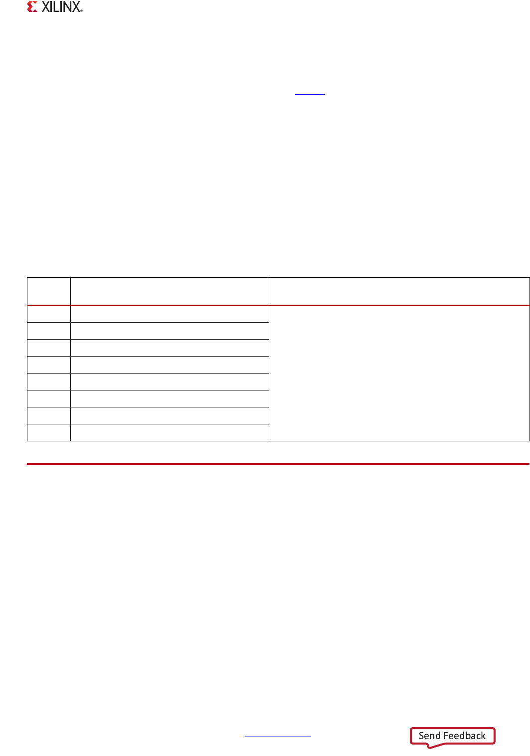
The alarm signals are summarized in Table 30-1.
30.3 PS-XADC Interface Description
The main function of the PS-XADC interface is to serialize commands written by software before
sending them to the XADC, and to perform a serial-to-parallel conversion when serial data is received
from the XADC for the software to read.
30.3.1 Serial Channel Clock Frequency
The serial communications channel between the PS-XADC interface and the XADC should not be
clocked faster than 50 MHz. The serial clock is derived from the PCAP_2x clock generated by the PS
clock subsystem (refer to Chapter 25, Clocks). This clock has a nominal frequency of 200 MHz. A
configurable clock divider is controlled by the devcfg.XADCIF_CFG [TCLK_RATE] bit field to reduce
the PCAP_2x clock frequency to no more than 50 MHz.
XADC serial clock = PCAP_2x clock / [TCLK_RATE]
Table 30-1: XADC Alarm Signals
Alarm Description
Upper/Lower Threshold Control and Maximum/Minimum
Status Registers
ALM[0]
Programmable Temperature sensor alarm
Refer to the LogiCORE User Guide sections:
• Maximum and Minimum Status Registers
• Automatic Alarms
ALM[1]
V
CCINT
sensor alarm (PL internal voltage)
ALM[2]
V
CCAUX
sensor alarm (PL auxiliary voltage)
ALM[3]
V
CCBRAM
sensor alarm (PL BRAM voltage)
ALM[4]
V
CCPINT
sensor alarm (PS internal voltage)
ALM[5]
V
CCPAUX
sensor alarm (PS auxiliary voltage)
ALM[6]
V
CCO_DDR
sensor alarm (PS DDR I/O voltage)
OT Over-temperature Alarm