
User manual


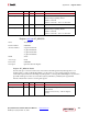


Table Of Contents
- Zynq-7000 All Programmable SoC
- Table of Contents
- Ch. 1: Introduction
- Ch. 2: Signals, Interfaces, and Pins
- Ch. 3: Application Processing Unit
- Ch. 4: System Addresses
- Ch. 5: Interconnect
- Ch. 6: Boot and Configuration
- Ch. 7: Interrupts
- Ch. 8: Timers
- Ch. 9: DMA Controller
- Introduction
- Functional Description
- DMA Transfers on the AXI Interconnect
- AXI Transaction Considerations
- DMA Manager
- Multi-channel Data FIFO (MFIFO)
- Memory-to-Memory Transfers
- PL Peripheral AXI Transactions
- PL Peripheral Request Interface
- PL Peripheral - Length Managed by PL Peripheral
- PL Peripheral - Length Managed by DMAC
- Events and Interrupts
- Aborts
- Security
- IP Configuration Options
- Programming Guide for DMA Controller
- Programming Guide for DMA Engine
- Programming Restrictions
- System Functions
- I/O Interface
- Ch. 10: DDR Memory Controller
- Introduction
- AXI Memory Port Interface (DDRI)
- DDR Core and Transaction Scheduler (DDRC)
- DDRC Arbitration
- Controller PHY (DDRP)
- Initialization and Calibration
- DDR Clock Initialization
- DDR IOB Impedance Calibration
- DDR IOB Configuration
- DDR Controller Register Programming
- DRAM Reset and Initialization
- DRAM Input Impedance (ODT) Calibration
- DRAM Output Impedance (RON) Calibration
- DRAM Training
- Write Data Eye Adjustment
- Alternatives to Automatic DRAM Training
- DRAM Write Latency Restriction
- Register Overview
- Error Correction Code (ECC)
- Programming Model
- Ch. 11: Static Memory Controller
- Ch. 12: Quad-SPI Flash Controller
- Ch. 13: SD/SDIO Controller
- Ch. 14: General Purpose I/O (GPIO)
- Ch. 15: USB Host, Device, and OTG Controller
- Introduction
- Functional Description
- Programming Overview and Reference
- Device Mode Control
- Device Endpoint Data Structures
- Device Endpoint Packet Operational Model
- Device Endpoint Descriptor Reference
- Programming Guide for Device Controller
- Programming Guide for Device Endpoint Data Structures
- Host Mode Data Structures
- EHCI Implementation
- Host Data Structures Reference
- Programming Guide for Host Controller
- OTG Description and Reference
- System Functions
- I/O Interfaces
- Ch. 16: Gigabit Ethernet Controller
- Ch. 17: SPI Controller
- Ch. 18: CAN Controller
- Ch. 19: UART Controller
- Ch. 20: I2C Controller
- Ch. 21: Programmable Logic Description
- Ch. 22: Programmable Logic Design Guide
- Ch. 23: Programmable Logic Test and Debug
- Ch. 24: Power Management
- Ch. 25: Clocks
- Ch. 26: Reset System
- Ch. 27: JTAG and DAP Subsystem
- Ch. 28: System Test and Debug
- Ch. 29: On-Chip Memory (OCM)
- Ch. 30: XADC Interface
- Ch. 31: PCI Express
- Ch. 32: Device Secure Boot
- Appx. A: Additional Resources
- Appx. B: Register Details
- Overview
- Acronyms
- Module Summary
- AXI_HP Interface (AFI) (axi_hp)
- CAN Controller (can)
- DDR Memory Controller (ddrc)
- CoreSight Cross Trigger Interface (cti)
- Performance Monitor Unit (cortexa9_pmu)
- CoreSight Program Trace Macrocell (ptm)
- Debug Access Port (dap)
- CoreSight Embedded Trace Buffer (etb)
- PL Fabric Trace Monitor (ftm)
- CoreSight Trace Funnel (funnel)
- CoreSight Intstrumentation Trace Macrocell (itm)
- CoreSight Trace Packet Output (tpiu)
- Device Configuration Interface (devcfg)
- DMA Controller (dmac)
- Gigabit Ethernet Controller (GEM)
- General Purpose I/O (gpio)
- Interconnect QoS (qos301)
- NIC301 Address Region Control (nic301_addr_region_ctrl_registers)
- I2C Controller (IIC)
- L2 Cache (L2Cpl310)
- Application Processing Unit (mpcore)
- On-Chip Memory (ocm)
- Quad-SPI Flash Controller (qspi)
- SD Controller (sdio)
- System Level Control Registers (slcr)
- Static Memory Controller (pl353)
- SPI Controller (SPI)
- System Watchdog Timer (swdt)
- Triple Timer Counter (ttc)
- UART Controller (UART)
- USB Controller (usb)

Zynq-7000 AP SoC Technical Reference Manual www.xilinx.com 797
UG585 (v1.11) September 27, 2016
Appendix B: Register Details
Register (can) SRR
Register SRR Details
Writing to the Software Reset Register (SRR) places the CAN controller in Configuration mode. Once in
Configuration mode, the CAN controller drives recessive on the bus line and does not transmit or receive
messages. During power-up, CEN and SRST bits are '0' and CONFIG bit in the Status Register (SR) is '1.'
TXHPB_DATA1 0x00000048 32 rw 0x00000000 transmit high priority buffer
data word 1
TXHPB_DATA2
0x0000004C 32 rw 0x00000000 transmit high priority buffer
data word 2
RXFIFO_ID
0x00000050 32 ro x receive message fifo message
identifier
RXFIFO_DLC
0x00000054 32 rw x receive message fifo data length
code
RXFIFO_DATA1
0x00000058 32 rw x receive message fifo data word 1
RXFIFO_DATA2
0x0000005C 32 rw x receive message fifo data word 2
AFR
0x00000060 32 rw 0x00000000 Acceptance Filter Register
AFMR1
0x00000064 32 rw x Acceptance Filter Mask Register
1
AFIR1
0x00000068 32 rw x Acceptance Filter ID Register 1
AFMR2
0x0000006C 32 rw x Acceptance Filter Mask Register
2
AFIR2
0x00000070 32 rw x Acceptance Filter ID Register 2
AFMR3
0x00000074 32 rw x Acceptance Filter Mask Register
3
AFIR3
0x00000078 32 rw x Acceptance Filter ID Register 3
AFMR4
0x0000007C 32 rw x Acceptance Filter Mask Register
4
AFIR4
0x00000080 32 rw x Acceptance Filter ID Register 4
Name SRR
Relative Address 0x00000000
Absolute Address can0: 0xE0008000
can1: 0xE0009000
Width 32 bits
Access Type rw
Reset Value 0x00000000
Description Software Reset Register
Register Name Address Width Type Reset Value Description