
User manual


Table Of Contents
- Zynq-7000 All Programmable SoC
- Table of Contents
- Ch. 1: Introduction
- Ch. 2: Signals, Interfaces, and Pins
- Ch. 3: Application Processing Unit
- Ch. 4: System Addresses
- Ch. 5: Interconnect
- Ch. 6: Boot and Configuration
- Ch. 7: Interrupts
- Ch. 8: Timers
- Ch. 9: DMA Controller
- Introduction
- Functional Description
- DMA Transfers on the AXI Interconnect
- AXI Transaction Considerations
- DMA Manager
- Multi-channel Data FIFO (MFIFO)
- Memory-to-Memory Transfers
- PL Peripheral AXI Transactions
- PL Peripheral Request Interface
- PL Peripheral - Length Managed by PL Peripheral
- PL Peripheral - Length Managed by DMAC
- Events and Interrupts
- Aborts
- Security
- IP Configuration Options
- Programming Guide for DMA Controller
- Programming Guide for DMA Engine
- Programming Restrictions
- System Functions
- I/O Interface
- Ch. 10: DDR Memory Controller
- Introduction
- AXI Memory Port Interface (DDRI)
- DDR Core and Transaction Scheduler (DDRC)
- DDRC Arbitration
- Controller PHY (DDRP)
- Initialization and Calibration
- DDR Clock Initialization
- DDR IOB Impedance Calibration
- DDR IOB Configuration
- DDR Controller Register Programming
- DRAM Reset and Initialization
- DRAM Input Impedance (ODT) Calibration
- DRAM Output Impedance (RON) Calibration
- DRAM Training
- Write Data Eye Adjustment
- Alternatives to Automatic DRAM Training
- DRAM Write Latency Restriction
- Register Overview
- Error Correction Code (ECC)
- Programming Model
- Ch. 11: Static Memory Controller
- Ch. 12: Quad-SPI Flash Controller
- Ch. 13: SD/SDIO Controller
- Ch. 14: General Purpose I/O (GPIO)
- Ch. 15: USB Host, Device, and OTG Controller
- Introduction
- Functional Description
- Programming Overview and Reference
- Device Mode Control
- Device Endpoint Data Structures
- Device Endpoint Packet Operational Model
- Device Endpoint Descriptor Reference
- Programming Guide for Device Controller
- Programming Guide for Device Endpoint Data Structures
- Host Mode Data Structures
- EHCI Implementation
- Host Data Structures Reference
- Programming Guide for Host Controller
- OTG Description and Reference
- System Functions
- I/O Interfaces
- Ch. 16: Gigabit Ethernet Controller
- Ch. 17: SPI Controller
- Ch. 18: CAN Controller
- Ch. 19: UART Controller
- Ch. 20: I2C Controller
- Ch. 21: Programmable Logic Description
- Ch. 22: Programmable Logic Design Guide
- Ch. 23: Programmable Logic Test and Debug
- Ch. 24: Power Management
- Ch. 25: Clocks
- Ch. 26: Reset System
- Ch. 27: JTAG and DAP Subsystem
- Ch. 28: System Test and Debug
- Ch. 29: On-Chip Memory (OCM)
- Ch. 30: XADC Interface
- Ch. 31: PCI Express
- Ch. 32: Device Secure Boot
- Appx. A: Additional Resources
- Appx. B: Register Details
- Overview
- Acronyms
- Module Summary
- AXI_HP Interface (AFI) (axi_hp)
- CAN Controller (can)
- DDR Memory Controller (ddrc)
- CoreSight Cross Trigger Interface (cti)
- Performance Monitor Unit (cortexa9_pmu)
- CoreSight Program Trace Macrocell (ptm)
- Debug Access Port (dap)
- CoreSight Embedded Trace Buffer (etb)
- PL Fabric Trace Monitor (ftm)
- CoreSight Trace Funnel (funnel)
- CoreSight Intstrumentation Trace Macrocell (itm)
- CoreSight Trace Packet Output (tpiu)
- Device Configuration Interface (devcfg)
- DMA Controller (dmac)
- Gigabit Ethernet Controller (GEM)
- General Purpose I/O (gpio)
- Interconnect QoS (qos301)
- NIC301 Address Region Control (nic301_addr_region_ctrl_registers)
- I2C Controller (IIC)
- L2 Cache (L2Cpl310)
- Application Processing Unit (mpcore)
- On-Chip Memory (ocm)
- Quad-SPI Flash Controller (qspi)
- SD Controller (sdio)
- System Level Control Registers (slcr)
- Static Memory Controller (pl353)
- SPI Controller (SPI)
- System Watchdog Timer (swdt)
- Triple Timer Counter (ttc)
- UART Controller (UART)
- USB Controller (usb)
Zynq-7000 AP SoC Technical Reference Manual www.xilinx.com 849
UG585 (v1.11) September 27, 2016
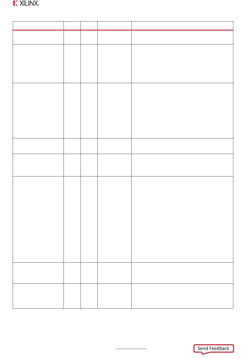
Appendix B: Register Details
reg_phy_mode_ddr1_d
dr2
29 rw 0x1 unused
reg_ddrc_read_latency 28:24 rw 0x5 Non-LPDDR2: not used.
DDR2 and DDR3: Set to Read Latency, RL. Time
from Read command to Read data on DRAM
interface. It is used to calculate when DRAM clock
may be stopped.
Unit: DDR clock.
reg_ddrc_en_dfi_dram
_clk_disable
23 rw 0x0 Enables the assertion of
ddrc_dfi_dram_clk_disable.
In DDR2/DDR3, only asserted in Self Refresh.
In mDDR/LPDDR2, can be asserted in following:
- during normal operation (Clock Stop),
- in Power Down
- in Self Refresh
- In Deep Power Down
reg_ddrc_mobile 22 rw 0x0 0: DDR2 or DDR3 device.
1: LPDDR2 device.
reg_ddrc_sdram 21 rw 0x0 1: sdram device
0: non-sdram device
Must be set to '1'.
reg_ddrc_refresh_to_x3
2
20:16 rw 0x8 If the refresh timer (tRFC_nom, as known as
tREFI) has expired at least once, but it has not
expired burst_of_N_refresh times yet, then a
'speculative refresh' may be performed. A
speculative refresh is a refresh performed at a
time when refresh would be useful, but before it is
absolutely required. When the DRAM bus is idle
for a period of time determined by this refresh
idle timeout and the refresh timer has expired at
least once since the last refresh, then a 'speculative
refresh' will be performed. Speculative refreshes
will continue successively until there are no
refreshes pending or until new reads or writes are
issued to the controller.
Dynamic Bit Field.
reg_ddrc_t_rp 15:12 rw 0x8 tRP - Minimum time from precharge to activate of
same bank.
DRAM RELATED
reg_ddrc_refresh_marg
in
11:8 rw 0x2 Issue critical refresh or page close this many
cycles before the critical refresh or page timer
expires. It is recommended that this not be
changed from the default value.
Field Name Bits Type Reset Value Description