
User manual


Table Of Contents
- Zynq-7000 All Programmable SoC
- Table of Contents
- Ch. 1: Introduction
- Ch. 2: Signals, Interfaces, and Pins
- Ch. 3: Application Processing Unit
- Ch. 4: System Addresses
- Ch. 5: Interconnect
- Ch. 6: Boot and Configuration
- Ch. 7: Interrupts
- Ch. 8: Timers
- Ch. 9: DMA Controller
- Introduction
- Functional Description
- DMA Transfers on the AXI Interconnect
- AXI Transaction Considerations
- DMA Manager
- Multi-channel Data FIFO (MFIFO)
- Memory-to-Memory Transfers
- PL Peripheral AXI Transactions
- PL Peripheral Request Interface
- PL Peripheral - Length Managed by PL Peripheral
- PL Peripheral - Length Managed by DMAC
- Events and Interrupts
- Aborts
- Security
- IP Configuration Options
- Programming Guide for DMA Controller
- Programming Guide for DMA Engine
- Programming Restrictions
- System Functions
- I/O Interface
- Ch. 10: DDR Memory Controller
- Introduction
- AXI Memory Port Interface (DDRI)
- DDR Core and Transaction Scheduler (DDRC)
- DDRC Arbitration
- Controller PHY (DDRP)
- Initialization and Calibration
- DDR Clock Initialization
- DDR IOB Impedance Calibration
- DDR IOB Configuration
- DDR Controller Register Programming
- DRAM Reset and Initialization
- DRAM Input Impedance (ODT) Calibration
- DRAM Output Impedance (RON) Calibration
- DRAM Training
- Write Data Eye Adjustment
- Alternatives to Automatic DRAM Training
- DRAM Write Latency Restriction
- Register Overview
- Error Correction Code (ECC)
- Programming Model
- Ch. 11: Static Memory Controller
- Ch. 12: Quad-SPI Flash Controller
- Ch. 13: SD/SDIO Controller
- Ch. 14: General Purpose I/O (GPIO)
- Ch. 15: USB Host, Device, and OTG Controller
- Introduction
- Functional Description
- Programming Overview and Reference
- Device Mode Control
- Device Endpoint Data Structures
- Device Endpoint Packet Operational Model
- Device Endpoint Descriptor Reference
- Programming Guide for Device Controller
- Programming Guide for Device Endpoint Data Structures
- Host Mode Data Structures
- EHCI Implementation
- Host Data Structures Reference
- Programming Guide for Host Controller
- OTG Description and Reference
- System Functions
- I/O Interfaces
- Ch. 16: Gigabit Ethernet Controller
- Ch. 17: SPI Controller
- Ch. 18: CAN Controller
- Ch. 19: UART Controller
- Ch. 20: I2C Controller
- Ch. 21: Programmable Logic Description
- Ch. 22: Programmable Logic Design Guide
- Ch. 23: Programmable Logic Test and Debug
- Ch. 24: Power Management
- Ch. 25: Clocks
- Ch. 26: Reset System
- Ch. 27: JTAG and DAP Subsystem
- Ch. 28: System Test and Debug
- Ch. 29: On-Chip Memory (OCM)
- Ch. 30: XADC Interface
- Ch. 31: PCI Express
- Ch. 32: Device Secure Boot
- Appx. A: Additional Resources
- Appx. B: Register Details
- Overview
- Acronyms
- Module Summary
- AXI_HP Interface (AFI) (axi_hp)
- CAN Controller (can)
- DDR Memory Controller (ddrc)
- CoreSight Cross Trigger Interface (cti)
- Performance Monitor Unit (cortexa9_pmu)
- CoreSight Program Trace Macrocell (ptm)
- Debug Access Port (dap)
- CoreSight Embedded Trace Buffer (etb)
- PL Fabric Trace Monitor (ftm)
- CoreSight Trace Funnel (funnel)
- CoreSight Intstrumentation Trace Macrocell (itm)
- CoreSight Trace Packet Output (tpiu)
- Device Configuration Interface (devcfg)
- DMA Controller (dmac)
- Gigabit Ethernet Controller (GEM)
- General Purpose I/O (gpio)
- Interconnect QoS (qos301)
- NIC301 Address Region Control (nic301_addr_region_ctrl_registers)
- I2C Controller (IIC)
- L2 Cache (L2Cpl310)
- Application Processing Unit (mpcore)
- On-Chip Memory (ocm)
- Quad-SPI Flash Controller (qspi)
- SD Controller (sdio)
- System Level Control Registers (slcr)
- Static Memory Controller (pl353)
- SPI Controller (SPI)
- System Watchdog Timer (swdt)
- Triple Timer Counter (ttc)
- UART Controller (UART)
- USB Controller (usb)
Zynq-7000 AP SoC Technical Reference Manual www.xilinx.com 886
UG585 (v1.11) September 27, 2016
Appendix B: Register Details
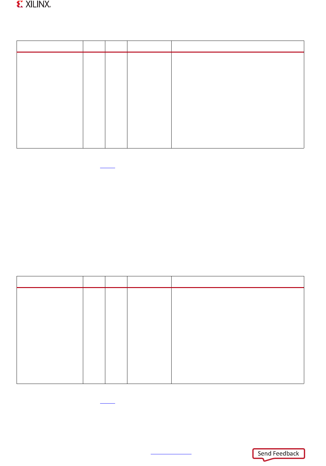
Register CHE_ECC_CORR_BIT_MASK_31_0_REG_OFFSET Details
Register (ddrc) CHE_ECC_CORR_BIT_MASK_63_32_REG_OFFSET
Register CHE_ECC_CORR_BIT_MASK_63_32_REG_OFFSET Details
Register (ddrc) phy_rcvr_enable
Field Name Bits Type Reset Value Description
ddrc_reg_ecc_corr_bit_
mask
31:0 ro 0x0 Bits [31:0] of ddrc_reg_ecc_corr_bit_mask
register. Indicates the mask of the corrected data.
1 - on any bit indicates that the bit has been
corrected by the DRAM ECC logic 0 - on any bit
indicates that the bit has NOT been corrected by
the DRAM ECC logic. Valid when any bit of
'ddrc_reg_ecc_corrected_err' is high. This mask
doesn't indicate any correction that has been
made in the ECC check bits. If there are errors in
multiple lanes, then this signal will have the mask
for the lowest lane. Each ECC engine works on
8-bits of data. Hence only the lower 8-bits carry
valid information. Upper 24-bits are always 0.
Name CHE_ECC_CORR_BIT_MASK_63_32_REG_OFFSET
Relative Address 0x000000FC
Absolute Address 0xF80060FC
Width 32 bits
Access Type ro
Reset Value 0x00000000
Description ECC data mask high
Field Name Bits Type Reset Value Description
ddrc_reg_ecc_corr_bit_
mask
31:0 ro 0x0 Bits [63:32] of ddrc_reg_ecc_corr_bit_mask
register. Indicates the mask of the corrected data.
1 - on any bit indicates that the bit has been
corrected by the DRAM ECC logic 0 - on any bit
indicates that the bit has NOT been corrected by
the DRAM ECC logic. Valid when any bit of
'ddrc_reg_ecc_corrected_err' is high. This mask
doesn't indicate any correction that has been
made in the ECC check bits. If there are errors in
multiple lanes, then this signal will have the mask
for the lowest lane. Each ECC engine works on
8-bits of data and this is reported in register 0x3E.
All 32-bits of this register are 0 always.
Name phy_rcvr_enable