
User manual


Table Of Contents
- Zynq-7000 All Programmable SoC
- Table of Contents
- Ch. 1: Introduction
- Ch. 2: Signals, Interfaces, and Pins
- Ch. 3: Application Processing Unit
- Ch. 4: System Addresses
- Ch. 5: Interconnect
- Ch. 6: Boot and Configuration
- Ch. 7: Interrupts
- Ch. 8: Timers
- Ch. 9: DMA Controller
- Introduction
- Functional Description
- DMA Transfers on the AXI Interconnect
- AXI Transaction Considerations
- DMA Manager
- Multi-channel Data FIFO (MFIFO)
- Memory-to-Memory Transfers
- PL Peripheral AXI Transactions
- PL Peripheral Request Interface
- PL Peripheral - Length Managed by PL Peripheral
- PL Peripheral - Length Managed by DMAC
- Events and Interrupts
- Aborts
- Security
- IP Configuration Options
- Programming Guide for DMA Controller
- Programming Guide for DMA Engine
- Programming Restrictions
- System Functions
- I/O Interface
- Ch. 10: DDR Memory Controller
- Introduction
- AXI Memory Port Interface (DDRI)
- DDR Core and Transaction Scheduler (DDRC)
- DDRC Arbitration
- Controller PHY (DDRP)
- Initialization and Calibration
- DDR Clock Initialization
- DDR IOB Impedance Calibration
- DDR IOB Configuration
- DDR Controller Register Programming
- DRAM Reset and Initialization
- DRAM Input Impedance (ODT) Calibration
- DRAM Output Impedance (RON) Calibration
- DRAM Training
- Write Data Eye Adjustment
- Alternatives to Automatic DRAM Training
- DRAM Write Latency Restriction
- Register Overview
- Error Correction Code (ECC)
- Programming Model
- Ch. 11: Static Memory Controller
- Ch. 12: Quad-SPI Flash Controller
- Ch. 13: SD/SDIO Controller
- Ch. 14: General Purpose I/O (GPIO)
- Ch. 15: USB Host, Device, and OTG Controller
- Introduction
- Functional Description
- Programming Overview and Reference
- Device Mode Control
- Device Endpoint Data Structures
- Device Endpoint Packet Operational Model
- Device Endpoint Descriptor Reference
- Programming Guide for Device Controller
- Programming Guide for Device Endpoint Data Structures
- Host Mode Data Structures
- EHCI Implementation
- Host Data Structures Reference
- Programming Guide for Host Controller
- OTG Description and Reference
- System Functions
- I/O Interfaces
- Ch. 16: Gigabit Ethernet Controller
- Ch. 17: SPI Controller
- Ch. 18: CAN Controller
- Ch. 19: UART Controller
- Ch. 20: I2C Controller
- Ch. 21: Programmable Logic Description
- Ch. 22: Programmable Logic Design Guide
- Ch. 23: Programmable Logic Test and Debug
- Ch. 24: Power Management
- Ch. 25: Clocks
- Ch. 26: Reset System
- Ch. 27: JTAG and DAP Subsystem
- Ch. 28: System Test and Debug
- Ch. 29: On-Chip Memory (OCM)
- Ch. 30: XADC Interface
- Ch. 31: PCI Express
- Ch. 32: Device Secure Boot
- Appx. A: Additional Resources
- Appx. B: Register Details
- Overview
- Acronyms
- Module Summary
- AXI_HP Interface (AFI) (axi_hp)
- CAN Controller (can)
- DDR Memory Controller (ddrc)
- CoreSight Cross Trigger Interface (cti)
- Performance Monitor Unit (cortexa9_pmu)
- CoreSight Program Trace Macrocell (ptm)
- Debug Access Port (dap)
- CoreSight Embedded Trace Buffer (etb)
- PL Fabric Trace Monitor (ftm)
- CoreSight Trace Funnel (funnel)
- CoreSight Intstrumentation Trace Macrocell (itm)
- CoreSight Trace Packet Output (tpiu)
- Device Configuration Interface (devcfg)
- DMA Controller (dmac)
- Gigabit Ethernet Controller (GEM)
- General Purpose I/O (gpio)
- Interconnect QoS (qos301)
- NIC301 Address Region Control (nic301_addr_region_ctrl_registers)
- I2C Controller (IIC)
- L2 Cache (L2Cpl310)
- Application Processing Unit (mpcore)
- On-Chip Memory (ocm)
- Quad-SPI Flash Controller (qspi)
- SD Controller (sdio)
- System Level Control Registers (slcr)
- Static Memory Controller (pl353)
- SPI Controller (SPI)
- System Watchdog Timer (swdt)
- Triple Timer Counter (ttc)
- UART Controller (UART)
- USB Controller (usb)
Zynq-7000 AP SoC Technical Reference Manual www.xilinx.com 94
UG585 (v1.11) September 27, 2016
Chapter 3: Application Processing Unit
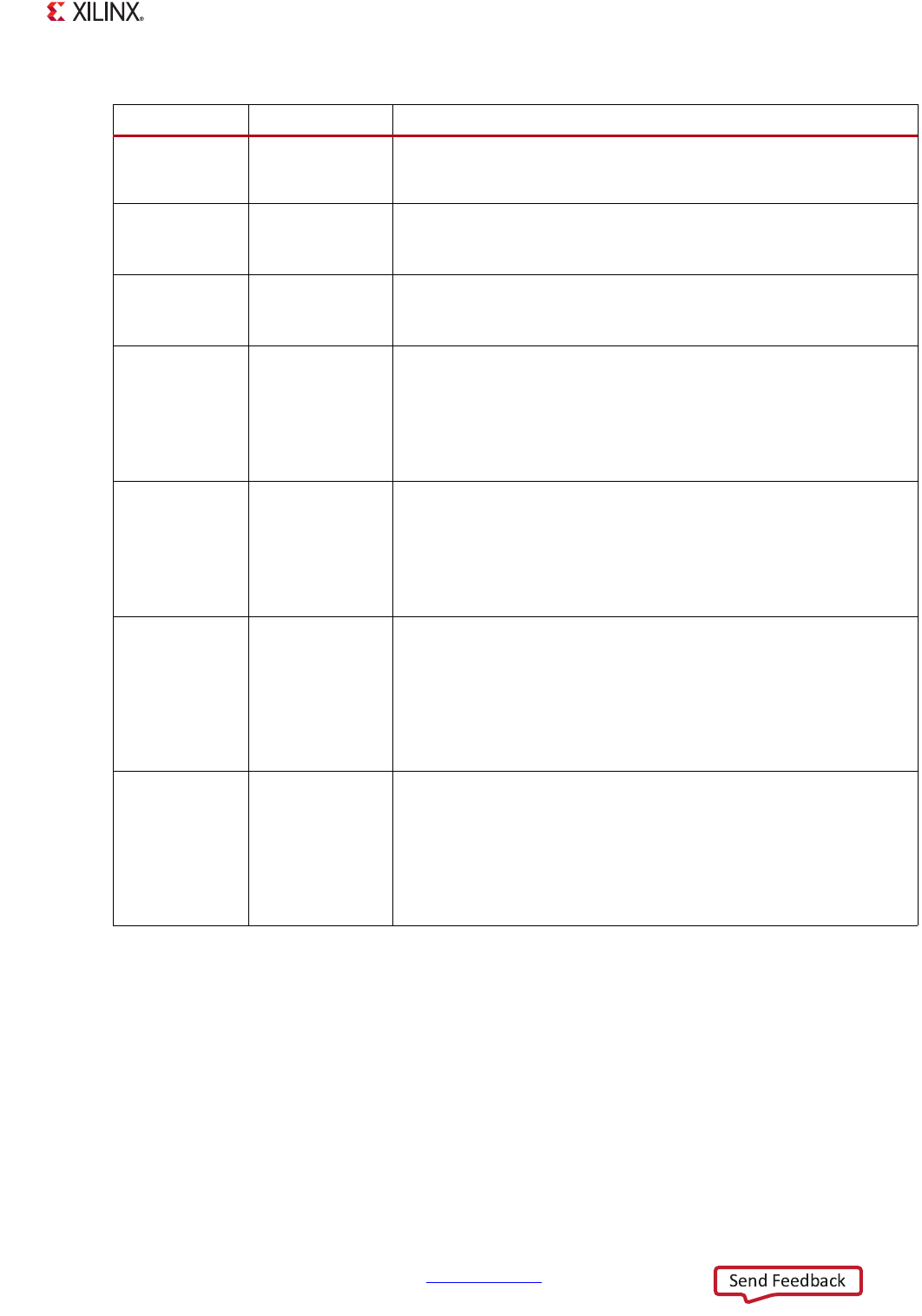
Table 3-5: Cache Controller Behavior for SCU Requests
Transaction Type ARMv7 Equivalent L2 Cache Controller Behavior
Non-cacheable
and
non-bufferable
Strongly ordered • Read: Not cached in L2, results in memory access.
• Write: Not buffered, results in memory access.
Bufferable only Device • Read: Not cached in L2, results in memory access.
• Write: Placed in store buffer, not merged, immediately drained to
memory.
Cacheable but
do not allocate
Outer
non-cacheable
• Read: Not cached in L2, results in memory access.
• Write: Placed in store buffer, write to memory when store buffer is
drained.
Cacheable
write-through,
allocate on read
Outer
write-through, no
write allocate
• Read hit: Read from L2.
• Read miss: Line fill to L2.
• Write hit: Put in store buffer, write to L2 and memory when store
buffer is drained.
• Write miss: Put in store buffer, write to memory when store buffer is
drained.
Cacheable
write-back,
allocate on read
Outer write-back,
no write allocate
• Read hit: Read from L2.
• Read miss: Line fill to L2.
• Write hit: Put in store buffer, write to L2 when store buffer is drained
and mark line as dirty.
• Write miss: Put in store buffer, write to memory when store buffer is
drained.
Cacheable
write-through,
allocate on write
-
• Read hit: Read from L2.
• Read miss: Not cached in L2, causes memory access.
• Write hit: Put in store buffer, write to L2 and memory when store
buffer is drained.
• Write miss: Put in store buffer. When buffer is drained, check if it is
full. If not full, request word or line to memory before allocating
buffer to L2. Allocation to L2. Write to memory.
Cacheable
write-back,
allocate on write
-
• Read hit: Read from L2.
• Read miss: Not cached in L2, causes memory access.
• Write hit: Put in store buffer, write to L2 when store buffer is drained,
and mark line as dirty.
• Write miss: Put in store buffer. When buffer has to be drained, check
if it is full. If it is not full then request word or line to memory before
allocating the buffer to L2. Allocation to L2.