
User manual


Table Of Contents
- Zynq-7000 All Programmable SoC
- Table of Contents
- Ch. 1: Introduction
- Ch. 2: Signals, Interfaces, and Pins
- Ch. 3: Application Processing Unit
- Ch. 4: System Addresses
- Ch. 5: Interconnect
- Ch. 6: Boot and Configuration
- Ch. 7: Interrupts
- Ch. 8: Timers
- Ch. 9: DMA Controller
- Introduction
- Functional Description
- DMA Transfers on the AXI Interconnect
- AXI Transaction Considerations
- DMA Manager
- Multi-channel Data FIFO (MFIFO)
- Memory-to-Memory Transfers
- PL Peripheral AXI Transactions
- PL Peripheral Request Interface
- PL Peripheral - Length Managed by PL Peripheral
- PL Peripheral - Length Managed by DMAC
- Events and Interrupts
- Aborts
- Security
- IP Configuration Options
- Programming Guide for DMA Controller
- Programming Guide for DMA Engine
- Programming Restrictions
- System Functions
- I/O Interface
- Ch. 10: DDR Memory Controller
- Introduction
- AXI Memory Port Interface (DDRI)
- DDR Core and Transaction Scheduler (DDRC)
- DDRC Arbitration
- Controller PHY (DDRP)
- Initialization and Calibration
- DDR Clock Initialization
- DDR IOB Impedance Calibration
- DDR IOB Configuration
- DDR Controller Register Programming
- DRAM Reset and Initialization
- DRAM Input Impedance (ODT) Calibration
- DRAM Output Impedance (RON) Calibration
- DRAM Training
- Write Data Eye Adjustment
- Alternatives to Automatic DRAM Training
- DRAM Write Latency Restriction
- Register Overview
- Error Correction Code (ECC)
- Programming Model
- Ch. 11: Static Memory Controller
- Ch. 12: Quad-SPI Flash Controller
- Ch. 13: SD/SDIO Controller
- Ch. 14: General Purpose I/O (GPIO)
- Ch. 15: USB Host, Device, and OTG Controller
- Introduction
- Functional Description
- Programming Overview and Reference
- Device Mode Control
- Device Endpoint Data Structures
- Device Endpoint Packet Operational Model
- Device Endpoint Descriptor Reference
- Programming Guide for Device Controller
- Programming Guide for Device Endpoint Data Structures
- Host Mode Data Structures
- EHCI Implementation
- Host Data Structures Reference
- Programming Guide for Host Controller
- OTG Description and Reference
- System Functions
- I/O Interfaces
- Ch. 16: Gigabit Ethernet Controller
- Ch. 17: SPI Controller
- Ch. 18: CAN Controller
- Ch. 19: UART Controller
- Ch. 20: I2C Controller
- Ch. 21: Programmable Logic Description
- Ch. 22: Programmable Logic Design Guide
- Ch. 23: Programmable Logic Test and Debug
- Ch. 24: Power Management
- Ch. 25: Clocks
- Ch. 26: Reset System
- Ch. 27: JTAG and DAP Subsystem
- Ch. 28: System Test and Debug
- Ch. 29: On-Chip Memory (OCM)
- Ch. 30: XADC Interface
- Ch. 31: PCI Express
- Ch. 32: Device Secure Boot
- Appx. A: Additional Resources
- Appx. B: Register Details
- Overview
- Acronyms
- Module Summary
- AXI_HP Interface (AFI) (axi_hp)
- CAN Controller (can)
- DDR Memory Controller (ddrc)
- CoreSight Cross Trigger Interface (cti)
- Performance Monitor Unit (cortexa9_pmu)
- CoreSight Program Trace Macrocell (ptm)
- Debug Access Port (dap)
- CoreSight Embedded Trace Buffer (etb)
- PL Fabric Trace Monitor (ftm)
- CoreSight Trace Funnel (funnel)
- CoreSight Intstrumentation Trace Macrocell (itm)
- CoreSight Trace Packet Output (tpiu)
- Device Configuration Interface (devcfg)
- DMA Controller (dmac)
- Gigabit Ethernet Controller (GEM)
- General Purpose I/O (gpio)
- Interconnect QoS (qos301)
- NIC301 Address Region Control (nic301_addr_region_ctrl_registers)
- I2C Controller (IIC)
- L2 Cache (L2Cpl310)
- Application Processing Unit (mpcore)
- On-Chip Memory (ocm)
- Quad-SPI Flash Controller (qspi)
- SD Controller (sdio)
- System Level Control Registers (slcr)
- Static Memory Controller (pl353)
- SPI Controller (SPI)
- System Watchdog Timer (swdt)
- Triple Timer Counter (ttc)
- UART Controller (UART)
- USB Controller (usb)
Zynq-7000 AP SoC Technical Reference Manual www.xilinx.com 97
UG585 (v1.11) September 27, 2016
Chapter 3: Application Processing Unit
32-bit cache address consists of the following fields: [Tag Field], [Index Field], [Word Field], [Byte
Field].
When a cache lookup occurs, the index defines where to look in the cache ways. The number of ways
defines the number of locations with the same index referred to as a set. Therefore, an 8-way set
associative cache has eight locations where an address with index A can exist. There are 2
11
or 2,048
indices in the 512K L2 cache.
Lockdown format C, as the ARM Architecture Reference Manual describes, provides a method to
restrict the replacement algorithm used for allocations of cache lines within a set. This method
enables:
• Fetch of code or load data into the L2 cache
• Protection from being evicted because of other accesses
• This method can also be used to reduce cache pollution.
The lockdown register in the L2 cache controller is used to lock any of the eight ways in the L2 cache.
To apply lockdown, you set each bit to 1 to lock each respective way. For example, set bit [0] for Way
0, bit [1] for Way 1.
Lockdown by Master
The lockdown by master feature is a superset of the lockdown by way feature. It enables multiple
masters to share the L2 cache and makes the L2 cache behave as though these masters have
dedicated smaller L2 caches. This feature enables you to reserve ways of the L2 cache to specific
master IDs.
There are eight Instruction and eight Data Lock-Down registers in the L2 cache controller
(0xF8F02900 to 0xF8F0293C) and each register is associated with one of the master IDs identified
by AR/WUSERSx[7:5] bits. Each register contains a 16-bit DATALOCK or INSTRLOCK field. By setting
any of the 16 bits in those fields to 1, the user can lock down that specific way for its corresponding
master ID.
The L2 cache controller lockdown by master is only able to distinguish up to eight different masters.
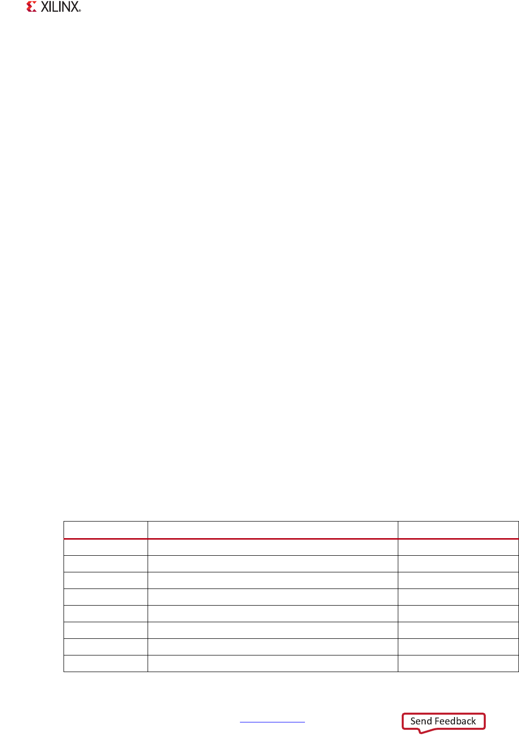
However, there are up to 64 AXI master IDs from the Cortex-A9 MP core. Table 3-6 shows how the 64
master ID values are grouped into eight lockable groups.
Table 3-6: Lockdown by Master ID Group
ID Group Transaction Sources L2 DATA/INSTRLOCKxxx
A9 Core 0 All read/write and instruction fetch requests from Core 0 000
A9 Core 1 All read/write and instruction fetch requests from Core 1 001
A9 Core 2 Reserved for future 010
A9 Core 3 Reserved for future 011
ACP Group0 ACP requests with ID = {000, 001} 100
ACP Group1 ACP requests with ID = {010, 011} 101
ACP Group2 ACP requests with ID = {100, 101} 110
ACP Group3 ACP requests with ID = {110, 111} 111