
Datasheet


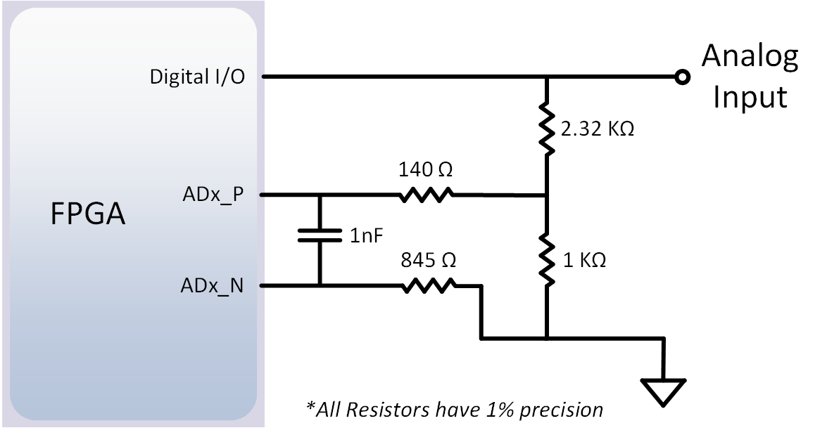
Arty S7's GND) that is applied to any of these pins. If you wish to use the pins labeled A0-A5 as
Digital inputs or outputs, they are also connected directly to the FPGA before the resistor divider
circuit (also shown in Figure 9.2.1).
Figure 9.2.1. Single-Ended Analog Inputs
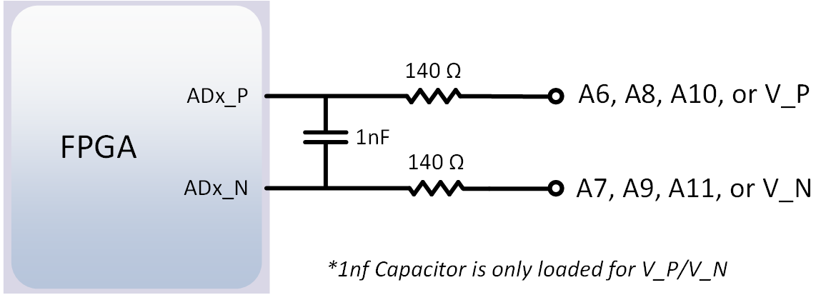
The pins labeled A6-A9 are connected directly to 2 pairs of analog capable pins on the FPGA via
an anti-aliasing filter. This circuit is shown in Figure 9.2.2. These pairs of pins can be used as
differential analog inputs with a voltage difference between 0-1V. The even numbers are connected
to the positive pins of the pair and the odd numbers are connected to the negative pins (so A6 and
A7 form an analog input pair with A6 being positive and A7 being negative). Note that though the
pads for the capacitor are present, they are not loaded for these pins. Since the analog capable
pins of the FPGA can also be used like normal digital FPGA pins, it is also possible to use these
pins for Digital I/O.
The pins labeled V_P and V_N are connected to the VP_0 and VN_0 dedicated analog inputs of
the FPGA. This pair of pins can also be used as a differential analog input with voltage between
0-1V, but they cannot be used as Digital I/O. The capacitor in the circuit shown in Figure 9.2.2 for
this pair of pins is loaded on the Arty S7.
Figure 9.2.2. Differential Analog Inputs