
Data Sheet


3/15/2018 Arty S7 Reference Manual [Reference.Digilentinc]
https://reference.digilentinc.com/reference/programmable-logic/arty-s7/reference-manual 20/22
Absolute
Minimum Voltage
Recommended Minimum
Operating Voltage
Recommended Maximum
Operating Voltage
Absolute
Maximum Voltage
Powered -0.4 V -0.2 V 3.4 V 3.75 V
Unpowered -0.4 V N/A N/A 0.55 V
Table 9.1.1. Shield Voltage Specifications
For more information on the electrical characteristics of the pins connected to the FPGA, please see the Spartan-7 datasheet
(https://www.xilinx.com/support/documentation/data_sheets/ds189-spartan-7-data-sheet.pdf) from Xilinx.
The pins on the shield connector typically used for I2C signals are labeled as SCL and SDA. When using these signals to implement an I2C
bus it is necessary to attach a pull-up resistor to them. On the Arty S7, this can be done by placing two shorting blocks horizontally across
the J4 header.
Pins A10 and A11 cannot be used as Digital I/O on the Arty S7-25. They are instead only to be used as
differential analog input pair.
The pins labeled A0-A9 and V_P/V_N are used as analog inputs to the XADC module of the FPGA. The FPGA expects that the inputs
range from 0-1 V. On the pins labeled A0-A5 we use an external circuit to scale down the input voltage from 3.3V. This circuit is shown in
Figure 9.2.1. This circuit allows the XADC module to accurately measure any voltage between 0V and 3.3V (relative to the Arty S7's GND
()) that is applied to any of these pins. If you wish to use the pins labeled A0-A5 as Digital inputs or outputs, they are also connected directly
to the FPGA before the resistor divider circuit (also shown in Figure 9.2.1).
(https://reference.digilentinc.com/_media/reference/programmable-logic/arty/arty_shield_analog_diff.png) Figure 9.2.1. Single-Ended Analog Inputs
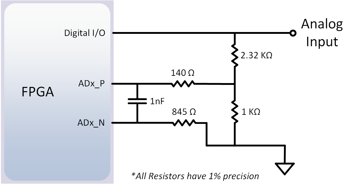
The pins labeled A6-A9 are connected directly to 2 pairs of analog capable pins on the FPGA via an anti-aliasing filter. This circuit is shown
in Figure 9.2.2. These pairs of pins can be used as differential analog inputs with a voltage difference between 0-1V. The even numbers are
connected to the positive pins of the pair and the odd numbers are connected to the negative pins (so A6 and A7 form an analog input pair
with A6 being positive and A7 being negative). Note that though the pads for the capacitor are present, they are not loaded for these pins.
Since the analog capable pins of the FPGA can also be used like normal digital FPGA pins, it is also possible to use these pins for Digital
I/O.
Pins A10 and A11 can only be used as a differential analog input pair on the Arty S7-25. They are not to be
used as Digital I/O.
Important!
9.2 Shield Analog I/O
Important!