Digilent FPGA PREVIEW: Arty S7 Spartan‐7 FPGA for Makers and Hobbyists SKU: 410‐352 Product Description The Arty S7 board features new Xilinx Spartan‐7 FPGA and is the latest member of the Arty family for Makers and Hobbyists. The Spartan‐7 FPGA offers the most size, performance, and cost‐conscious design engineered with the latest technologies from Xilinx and is fully compatible with Vivado Design Suite.
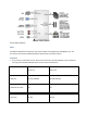
Arty S7 block diagram. Note: The official distribution channel for the Arty S7 board is through Avnet and Digilent only. For this reason, we cannot provide distributor discounts for the Arty S7 board. Features: Arty S7 comes in two FPGA variants: Arty S7‐25 features Xilinx XC7S25‐CSGA324. Arty S7‐50 features the larger Xilinx XC7S50‐CSGA324.
Slices 3,650 8,150 Flip‐flops 29,200 65,200 Block RAM (Kbits) 1,620 2,700 Clock Management Tiles 3 5 DSP Slices 80 120 Internal clock speeds exceeding 450MHz; On‐chip analog‐to‐digital converter (XADC). Programmable over JTAG and Quad‐SPI Flash System Features: o 256 MB DDR3L with a 16‐bit bus @ 667 MHz o 128 Mbits Quad‐SPI Flash o 100 MHz External Clock o USB‐JTAG Programming circuitry (USB Micro cable required, NOT INCLUDED).
What's Included: Arty S7 Board Spartan‐7 FPGA Digilent cardboard packaging with protective foam http://store.digilentinc.
18 7 Series FPGAs Data Sheet: Overview DS180 (v2.5) August 1, 2017 Product Specification General Description Xilinx® 7 series FPGAs comprise four FPGA families that address the complete range of system requirements, ranging from low cost, small form factor, cost-sensitive, high-volume applications to ultra high-end connectivity bandwidth, logic capacity, and signal processing capability for the most demanding high-performance applications.
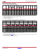
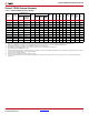
7 Series FPGAs Data Sheet: Overview Spartan-7 FPGA Feature Summary Table 2: Spartan-7 FPGA Feature Summary by Device Block RAM Blocks(3) CLB Device Logic Cells Slices(1) Max Distributed RAM (Kb) DSP Slices(2) 18 Kb 36 Kb Max (Kb) 180 CMTs(4) PCIe GT XADC Blocks Total I/O Banks(5) Max User I/O 2 0 0 0 2 100 XC7S6 6,000 938 70 10 10 5 XC7S15 12,800 2,000 150 20 20 10 360 2 0 0 0 2 100 XC7S25 23,360 3,650 313 80 90 45 1,620 3 0 0 1 3 150 XC7S50 52,160
Series FPGAs Data Sheet: Overview Artix-7 FPGA Feature Summary Table 4: Artix-7 FPGA Feature Summary by Device Configurable Logic Blocks (CLBs) Device Logic Cells Slices(1) Max Distributed RAM (Kb) Block RAM Blocks(3) DSP48E1 Slices(2) 18 Kb 36 Kb Max (Kb) CMTs(4) PCIe(5) GTPs XADC Blocks Total I/O Banks(6) Max User I/O(7) XC7A12T 12,800 2,000 171 40 40 20 720 3 1 2 1 3 150 XC7A15T 16,640 2,600 200 45 50 25 900 5 1 4 1 5 250 XC7A25T 23,360 3,650 313 80 90 45
7 Series FPGAs Data Sheet: Overview Kintex-7 FPGA Feature Summary Table 6: Kintex-7 FPGA Feature Summary by Device Configurable Logic Blocks (CLBs) Device Logic Cells Block RAM Blocks(3) Max Distributed RAM (Kb) Slices(1) DSP Slices(2) CMTs(4) 18 Kb 36 Kb PCIe(5) GTXs XADC Blocks Total I/O Banks(6) Max (Kb) Max User I/O(7) XC7K70T 65,600 10,250 838 240 270 135 4,860 6 1 8 1 6 300 XC7K160T 162,240 25,350 2,188 600 650 325 11,700 8 1 8 1 8 400 XC7K325T 326,080 50,9
7 Series FPGAs Data Sheet: Overview Virtex-7 FPGA Feature Summary Table 8: Virtex-7 FPGA Feature Summary Configurable Logic Blocks (CLBs) Device(1) Logic Cells Slices(2) Max Distributed RAM (Kb) Block RAM Blocks(4) DSP Slices(3) 18 Kb 36 Kb Max (Kb) CMTs PCIe (6) GTX GTH GTZ XADC Blocks Total I/O Banks(7) Max User I/O(8) SLRs(9) 0 0 1 17 850 N/A (5) XC7V585T 582,720 91,050 6,938 1,260 1,590 795 28,620 18 3 36 XC7V2000T 1,954,560 305,400 21,550 2,160 2,584 1,292 46,5
7 Series FPGAs Data Sheet: Overview Table 9: Virtex-7 FPGA Device-Package Combinations and Maximum I/Os Package(1) FFG1157 FFG1761(2) FHG1761(2) FLG1925 Size (mm) 35 x 35 42.5 x 42.5 45 x 45 45 x 45 Ball Pitch 1.0 1.0 1.0 I/O Device XC7V585T GTX GTH 20 0 HR(3) HP(4) 0 1.
7 Series FPGAs Data Sheet: Overview Table 11: Virtex-7 HT FPGA Device-Package Combinations and Maximum I/Os Package(1) FLG1155 FLG1931 FLG1932 Size (mm) 35 x 35 45 x 45 45 x 45 Ball Pitch 1.0 1.0 I/O Device XC7VH580T GTH GTZ 24 8 HP(2) 1.0 I/O GTH GTZ 48 8 400 HP(2) I/O GTH GTZ 72 16 HP(2) 600 XC7VH870T 300 Notes: 1. All packages listed are Pb-free with exemption 15. Some packages are available in Pb option. 2. HP = High-performance I/O with support for I/O voltage from 1.
7 Series FPGAs Data Sheet: Overview Mixed-Mode Clock Manager and Phase-Locked Loop The MMCM and PLL share many characteristics. Both can serve as a frequency synthesizer for a wide range of frequencies and as a jitter filter for incoming clocks. At the center of both components is a voltage-controlled oscillator (VCO), which speeds up and slows down depending on the input voltage it receives from the phase frequency detector (PFD). There are three sets of programmable frequency dividers: D, M, and O.
7 Series FPGAs Data Sheet: Overview Block RAM Some of the key features of the block RAM include: • Dual-port 36 Kb block RAM with port widths of up to 72 • Programmable FIFO logic • Built-in optional error correction circuitry Every 7 series FPGA has between 5 and 1,880 dual-port block RAMs, each storing 36 Kb. Each block RAM has two completely independent ports that share nothing but the stored data. Synchronous Operation Each memory access, read or write, is controlled by the clock.
7 Series FPGAs Data Sheet: Overview Digital Signal Processing — DSP Slice Some highlights of the DSP functionality include: • 25 × 18 two's complement multiplier/accumulator high-resolution (48 bit) signal processor • Power saving pre-adder to optimize symmetrical filter applications • Advanced features: optional pipelining, optional ALU, and dedicated buses for cascading DSP applications use many binary multipliers and accumulators, best implemented in dedicated DSP slices.
7 Series FPGAs Data Sheet: Overview I/O Electrical Characteristics Single-ended outputs use a conventional CMOS push/pull output structure driving High towards VCCO or Low towards ground, and can be put into a high-Z state. The system designer can specify the slew rate and the output strength. The input is always active but is usually ignored while the output is active. Each pin can optionally have a weak pull-up or a weak pulldown resistor.
7 Series FPGAs Data Sheet: Overview LC tank or, in the case of the GTZ, a single LC tank architecture to allow the ideal blend of flexibility and performance while enabling IP portability across the family members. The different 7 series family members offer different top-end data rates. The GTP operates up to 6.6 Gb/s, the GTX operates up to 12.5 Gb/s, the GTH operates up to 13.1 Gb/s, and the GTZ operates up to 28.05 Gb/s. Lower data rates can be achieved using FPGA logic-based oversampling.
7 Series FPGAs Data Sheet: Overview maximum payload size of up to 1,024 bytes. The integrated block interfaces to the integrated high-speed transceivers for serial connectivity and to block RAMs for data buffering. Combined, these elements implement the Physical Layer, Data Link Layer, and Transaction Layer of the PCI Express protocol.
7 Series FPGAs Data Sheet: Overview Encryption, Readback, and Partial Reconfiguration In all 7 series FPGAs (except XC7S6 and XC7S15), the FPGA bitstream, which contains sensitive customer IP, can be protected with 256-bit AES encryption and HMAC/SHA-256 authentication to prevent unauthorized copying of the design. The FPGA performs decryption on the fly during configuration using an internally stored 256-bit key. This key can reside in battery-backed RAM or in nonvolatile eFUSE bits.
7 Series FPGAs Data Sheet: Overview 7 Series FPGA Ordering Information Table 12 shows the speed and temperature grades available in the different device families. Some devices might not be available in every speed and temperature grade. Table 12: 7 Series Speed Grade and Temperature Ranges Device Family Speed Grade, Temperature Range, and Operating Voltage Devices Commercial (C) 0°C to +85°C Extended (E) 0°C to +100°C All Expanded (Q) –40°C to +125°C -2I (1.0V) -2C (1.
7 Series FPGAs Data Sheet: Overview The Spartan-7 FPGA ordering information is shown in Figure 1. Refer to the Package Marking section of UG475, 7 Series FPGAs Packaging and Pinout for a more detailed explanation of the device markings.
7 Series FPGAs Data Sheet: Overview Revision History The following table shows the revision history for this document: Date Version 06/21/10 1.0 Initial Xilinx release. 07/30/10 1.1 Added SHA-256 to authentication information. Updated Table 5, Table 7, Virtex-7 FPGA DevicePackage Combinations and Maximum I/Os table (Virtex-7 T devices), and Table 9 with ball pitch information and voltage bank information. Updated DSP and Logic Slice information in Table 8. Updated Low-Power Gigabit Transceivers.
7 Series FPGAs Data Sheet: Overview Date Version Description of Revisions 03/02/12 1.10 Updated General Description, Table 5, and Table 12. 05/02/12 1.11 Updated Table 7, Table 9, Table 10, Low-Power Gigabit Transceivers, and 7 Series FPGA Ordering Information. Added 7 Series FPGA Ordering Information. 10/15/12 1.12 Updated overview with Artix-7 SL and SLT devices. Updated Table 1, Table 4, Table 5, Table 8, Table 9, Table 10, Table 11, and Table 12. Added Table 3.
Spartan-7 FPGAs Data Sheet: DC and AC Switching Characteristics DS189 (v1.2) June 20, 2017 Preliminary Product Specification Introduction Spartan®-7 FPGAs are available in -2, -1, and -1L speed grades, with -2 having the highest performance. The Spartan-7 FPGAs predominantly operate at a 1.0V core voltage. The -1L devices are screened for lower maximum static power and can operate at lower core voltages for lower dynamic power than the -1 devices. The -1L devices operate only at VCCINT = VCCBRAM = 0.
Spartan-7 FPGAs Data Sheet: DC and AC Switching Characteristics Table 1: Absolute Maximum Ratings(1) (Cont’d) Symbol Description Min Max Units XADC VCCADC XADC supply relative to GNDADC. –0.5 2.0 V VREFP XADC reference input relative to GNDADC. –0.5 2.0 V –65 150 °C – +220 °C – +260 °C – +125 °C Temperature TSTG TSOL Storage temperature (ambient). Maximum soldering temperature for Pb/Sn component Maximum soldering temperature for Pb-free component Maximum junction temperature.
Spartan-7 FPGAs Data Sheet: DC and AC Switching Characteristics Table 2: Recommended Operating Conditions(1)(2) Symbol Description Min Typ Max Units For -2 and -1 (1.0V) devices: internal supply voltage. 0.95 1.00 1.05 V For -1L (0.95V) devices: internal supply voltage. 0.92 0.95 0.98 V Auxiliary supply voltage. 1.71 1.80 1.89 V For -2 and -1 (1.0V) devices: block RAM supply voltage. 0.95 1.00 1.05 V For -1L (0.95V) devices: block RAM supply voltage. 0.92 0.95 0.
Spartan-7 FPGAs Data Sheet: DC and AC Switching Characteristics Table 3: DC Characteristics Over Recommended Operating Conditions Symbol Description Min Typ(1) Max Units VDRINT Data retention VCCINT voltage (below which configuration data might be lost). 0.75 – – V VDRI Data retention VCCAUX voltage (below which configuration data might be lost). 1.5 – – V IREF VREF leakage current per pin. – – 15 µA IL Input or output leakage current per pin (sample-tested).
Spartan-7 FPGAs Data Sheet: DC and AC Switching Characteristics Table 4: VIN Maximum Allowed AC Voltage Overshoot and Undershoot for HR I/O Banks(1)(2) AC Voltage Overshoot % of UI at –40°C to 100°C VCCO + 0.55 AC Voltage Undershoot % of UI at –40°C to 100°C –0.40 100 –0.45 61.7 –0.50 25.8 –0.55 11.0 100 VCCO + 0.60 46.6 –0.60 4.77 VCCO + 0.65 21.2 –0.65 2.10 VCCO + 0.70 9.75 –0.70 0.94 VCCO + 0.75 4.55 –0.75 0.43 VCCO + 0.80 2.15 –0.80 0.20 VCCO + 0.85 1.02 –0.85 0.
Spartan-7 FPGAs Data Sheet: DC and AC Switching Characteristics Table 5: Typical Quiescent Supply Current(1)(2)(3) (Cont’d) Speed Grade Symbol Description Device 1.0V -2C/-2I ICCBRAMQ Quiescent VCCBRAM supply current. 0.95V -1C/-1I Units -1LI XC7S6 mA XC7S15 mA XC7S25 2 2 1 mA XC7S50 2 2 1 mA XC7S75 mA XC7S100 mA Notes: 1. 2. 3. Typical values are specified at nominal voltage, 85°C junction temperature (Tj) with single-ended SelectIO™ resources.
Spartan-7 FPGAs Data Sheet: DC and AC Switching Characteristics Table 6 shows the minimum current, in addition to I CCQ maximum, that is required by Spartan-7 devices for proper power-on and configuration. If the current minimums shown in Table 6 are met, the device powers on after all four supplies have passed through their power-on reset threshold voltages. The FPGA must not be configured until after VCCINT is applied.
Spartan-7 FPGAs Data Sheet: DC and AC Switching Characteristics DC Input and Output Levels Values for VIL and VIH are recommended input voltages. Values for IOL and IOH are guaranteed over the recommended operating conditions at the VOL and V OH test points. Only selected standards are tested. These are chosen to ensure that all standards meet their specifications. The selected standards are tested at a minimum V CCO with the respective VOL and VOH voltage levels shown. Other standards are sample tested.
Spartan-7 FPGAs Data Sheet: DC and AC Switching Characteristics Table 9: Differential SelectIO DC Input and Output Levels VICM(1) I/O Standard V, Typ V, Max V, Min VOCM(3) VOD(4) V, Typ V, Max V, Min V, Typ V, Max – – – 1.250 – Note 5 MINI_LVDS_25 0.300 1.200 VCCAUX 0.200 0.400 0.600 1.000 1.200 1.400 0.300 0.450 0.600 PPDS_25 0.200 0.900 VCCAUX 0.100 0.250 0.400 0.500 0.950 1.400 0.100 0.250 0.400 RSDS_25 0.300 0.900 1.500 0.100 0.350 0.600 1.000 1.200 1.400 0.100 0.350 0.
Spartan-7 FPGAs Data Sheet: DC and AC Switching Characteristics LVDS DC Specifications (LVDS_25) Table 11: LVDS_25 DC Specifications(1) Symbol DC Parameter Conditions Min Typ Max Units 2.375 2.500 2.625 V VCCO Supply voltage. VOH Output High voltage for Q and Q. RT = 100Ω across Q and Q signals. – – 1.675 V VOL Output Low voltage for Q and Q. RT = 100Ω across Q and Q signals. 0.700 – – V RT = 100Ω across Q and Q signals. 247 350 600 mV RT = 100Ω across Q and Q signals. 1.
Spartan-7 FPGAs Data Sheet: DC and AC Switching Characteristics AC Switching Characteristics All values represented in this data sheet are based on the speed specifications from the Vivado® Design Suite as outlined in Table 12. Table 12: Speed Specification Version By Device 2017.2 1.17 Device XC7S6, XC7S15, XC7S25, XC7S50, XC7S75, XC7S100 Switching characteristics are specified on a per-speed-grade basis and can be designated as Advance, Preliminary, or Production.
Spartan-7 FPGAs Data Sheet: DC and AC Switching Characteristics Speed Grade Designations Since individual family members are produced at different times, the migration from one category to another depends completely on the status of the fabrication process for each device. Table 13 correlates the current status of each Spartan-7 device on a per speed grade basis.
Spartan-7 FPGAs Data Sheet: DC and AC Switching Characteristics Performance Characteristics This section provides the performance characteristics of some common functions and designs implemented in Spartan-7 FPGAs. These values are subject to the same guidelines as the AC Switching Characteristics, page 11. Table 15: Networking Applications Interface Performances VCCINT Operating Voltage, Speed Grade, and Temperature Range Description 1.
Spartan-7 FPGAs Data Sheet: DC and AC Switching Characteristics IOB Pad Input/Output/3-State Table 17 summarizes the values of standard-specific data input delay adjustments, output delays terminating at pads (based on standard) and 3-state delays. • TIOPI is described as the delay from IOB pad through the input buffer to the I-pin of an IOB pad. The delay varies depending on the capability of the SelectIO input buffer.
Spartan-7 FPGAs Data Sheet: DC and AC Switching Characteristics Table 17: IOB High Range (HR) Switching Characteristics (Cont’d) TIOPI TIOOP TIOTP VCCINT Operating Voltage and Speed Grade I/O Standard 1.0V 0.95V 1.0V 0.95V 1.0V 0.95V Units -2 -1 -1L -2 -1 -1L -2 -1 -1L DIFF_MOBILE_DDR_F 0.78 0.85 0.85 1.57 1.82 1.82 1.60 1.84 1.84 ns HSTL_I_S 0.75 0.82 0.82 1.74 1.99 1.99 1.77 2.01 2.01 ns HSTL_II_S 0.73 0.80 0.80 1.54 1.79 1.79 1.57 1.80 1.
Spartan-7 FPGAs Data Sheet: DC and AC Switching Characteristics Table 17: IOB High Range (HR) Switching Characteristics (Cont’d) TIOPI TIOOP TIOTP VCCINT Operating Voltage and Speed Grade I/O Standard 1.0V 0.95V 1.0V 0.95V 1.0V 0.95V Units -2 -1 -1L -2 -1 -1L -2 -1 -1L LVCMOS18_S16 0.83 0.89 0.89 1.65 1.90 1.90 1.68 1.91 1.91 ns LVCMOS18_S24 0.83 0.89 0.89 1.72 1.98 1.98 1.75 1.99 1.99 ns LVCMOS18_F4 0.83 0.89 0.89 1.57 1.82 1.82 1.60 1.84 1.
Spartan-7 FPGAs Data Sheet: DC and AC Switching Characteristics Table 17: IOB High Range (HR) Switching Characteristics (Cont’d) TIOPI TIOOP TIOTP VCCINT Operating Voltage and Speed Grade I/O Standard 1.0V 0.95V 1.0V 0.95V 1.0V 0.95V Units -2 -1 -1L -2 -1 -1L -2 -1 -1L DIFF_SSTL18_I_F 0.79 0.86 0.86 1.35 1.60 1.60 1.38 1.62 1.62 ns DIFF_SSTL18_II_F 0.79 0.86 0.86 1.33 1.59 1.59 1.36 1.60 1.60 ns Table 18 specifies the values of T IOTPHZ and TIOIBUFDISABLE .
Spartan-7 FPGAs Data Sheet: DC and AC Switching Characteristics Table 19: Input Delay Measurement Methodology (Cont’d) Description I/O Standard Attribute VL(1) VH(1) VMEAS(3)(5) VREF(2)(4) HSUL (high-speed unterminated logic), 1.2V HSUL_12 VREF – 0.5 VREF + 0.5 VREF 0.60 SSTL (stub-terminated transceiver logic), 1.2V SSTL12 VREF – 0.5 VREF + 0.5 VREF 0.60 SSTL, 1.35V SSTL135, SSTL135_R VREF – 0.575 VREF + 0.575 VREF 0.675 SSTL, 1.5V SSTL15, SSTL15_R VREF – 0.65 VREF + 0.
Spartan-7 FPGAs Data Sheet: DC and AC Switching Characteristics Output Delay Measurements Output delays are measured with short output traces. Standard termination was used for all testing. The propagation delay of the trace is characterized separately and subtracted from the final measurement, and is therefore not included in the generalized test setups shown in Figure 1 and Figure 2.
Spartan-7 FPGAs Data Sheet: DC and AC Switching Characteristics Table 20: Output Delay Measurement Methodology Description I/O Standard Attribute RREF (Ω) CREF(1) VMEAS (pF) (V) VREF (V) LVCMOS, 1.2V LVCMOS12 1M 0 0.6 0 LVCMOS, 1.5V LVCMOS15 1M 0 0.75 0 LVCMOS, 1.8V LVCMOS18 1M 0 0.9 0 LVCMOS, 2.5V LVCMOS25 1M 0 1.25 0 LVCMOS, 3.3V LVCMOS33 1M 0 1.65 0 LVTTL, 3.3V LVTTL 1M 0 1.65 0 PCI33, 3.3V PCI33_3 25 10 1.
Spartan-7 FPGAs Data Sheet: DC and AC Switching Characteristics Input/Output Logic Switching Characteristics Table 21: ILOGIC Switching Characteristics VCCINT Operating Voltage and Speed Grade Symbol Description 1.0V -2 0.95V -1 Units -1L Setup/Hold TICE1CK/TICKCE1 CE1 pin setup/hold with respect to CLK. 0.54/0.02 0.76/0.02 0.76/0.02 ns TISRCK/TICKSR SR pin setup/hold with respect to CLK. 0.70/0.01 1.13/0.01 1.13/0.01 ns TIDOCK/TIOCKD D pin setup/hold with respect to CLK without delay. 0.
Spartan-7 FPGAs Data Sheet: DC and AC Switching Characteristics Table 22: OLOGIC Switching Characteristics VCCINT Operating Voltage and Speed Grade Symbol Description 1.0V -2 0.95V -1 Units -1L Setup/Hold TODCK/TOCKD D1/D2 pins setup/hold with respect to CLK. 0.71/–0.11 0.84/–0.11 0.84/–0.11 ns TOOCECK/TOCKOCE OCE pin setup/hold with respect to CLK. 0.34/0.58 0.51/0.58 0.51/0.58 ns TOSRCK/TOCKSR SR pin setup/hold with respect to CLK. 0.44/0.21 0.80/0.21 0.80/0.
Spartan-7 FPGAs Data Sheet: DC and AC Switching Characteristics Input Serializer/Deserializer Switching Characteristics Table 23: ISERDES Switching Characteristics VCCINT Operating Voltage and Speed Grade Symbol Description 1.0V 0.95V -2 -1 -1L 0.02/0.15 0.02/0.17 0.02/0.17 Units Setup/Hold for Control Lines TISCCK_BITSLIP/ TISCKC_BITSLIP BITSLIP pin setup/hold with respect to CLKDIV. TISCCK_CE/ TISCKC_CE CE pin setup/hold with respect to CLK (for CE1). 0.50/–0.01 0.72/–0.01 0.72/–0.
Spartan-7 FPGAs Data Sheet: DC and AC Switching Characteristics Output Serializer/Deserializer Switching Characteristics Table 24: OSERDES Switching Characteristics VCCINT Operating Voltage and Speed Grade Symbol Description 1.0V 0.95V -2 -1 -1L 0.45/0.03 0.63/0.03 0.63/0.03 Units Setup/Hold TOSDCK_D/ TOSCKD_D D input setup/hold with respect to CLKDIV. TOSDCK_T/ TOSCKD_T T input setup/hold with respect to CLK. 0.73/–0.13 0.88/–0.13 0.88/–0.
Spartan-7 FPGAs Data Sheet: DC and AC Switching Characteristics Input/Output Delay Switching Characteristics Table 25: Input/Output Delay Switching Characteristics VCCINT Operating Voltage and Speed Grade Symbol Description 1.0V 0.95V -2 -1 -1L Units IDELAYCTRL TDLYCCO_RDY FIDELAYCTRL_REF Reset to ready for IDELAYCTRL. 3.67 3.67 3.67 µs Attribute REFCLK frequency = 200.00.(1) 200.00 200.00 200.00 MHz Attribute REFCLK frequency = 300.00.(1) 300.00 300.00 300.
Spartan-7 FPGAs Data Sheet: DC and AC Switching Characteristics Table 26: IO_FIFO Switching Characteristics VCCINT Operating Voltage and Speed Grade Symbol Description 1.0V 0.95V -2 -1 -1L Units IO_FIFO Clock to Out Delays TOFFCKO_DO RDCLK to Q outputs. 0.60 0.68 0.68 ns TCKO_FLAGS Clock to IO_FIFO flags. 0.61 0.77 0.77 ns 0.51/0.02 0.58/0.02 0.58/0.02 ns Setup/Hold TCCK_D/TCKC_D D inputs to WRCLK. TIFFCCK_WREN/ TIFFCKC_WREN WREN to WRCLK.
Spartan-7 FPGAs Data Sheet: DC and AC Switching Characteristics CLB Switching Characteristics Table 27: CLB Switching Characteristics VCCINT Operating Voltage and Speed Grade Symbol Description 1.0V 0.95V -2 -1 -1L Units Combinatorial Delays TILO An – Dn LUT address to A. 0.11 0.13 0.13 ns, Max TILO_2 An – Dn LUT address to AMUX/CMUX. 0.30 0.36 0.36 ns, Max TILO_3 An – Dn LUT address to BMUX_A. 0.46 0.55 0.55 ns, Max TITO An – Dn inputs to A – D Q outputs. 1.05 1.27 1.
Spartan-7 FPGAs Data Sheet: DC and AC Switching Characteristics CLB Distributed RAM Switching Characteristics (SLICEM Only) Table 28: CLB Distributed RAM Switching Characteristics VCCINT Operating Voltage and Speed Grade Symbol Description 1.0V 0.95V -2 -1 -1L Units Sequential Delays TSHCKO Clock to A – B outputs. 1.09 1.32 1.32 ns, Max TSHCKO_1 Clock to AMUX – BMUX outputs. 1.53 1.86 1.86 ns, Max Setup and Hold Times Before/After Clock CLK TDS_LRAM/TDH_LRAM A – D inputs to CLK. 0.
Spartan-7 FPGAs Data Sheet: DC and AC Switching Characteristics Block RAM and FIFO Switching Characteristics Table 30: Block RAM and FIFO Switching Characteristics VCCINT Operating Voltage and Speed Grade Symbol Description 1.0V 0.95V Units -2 -1 -1L Clock CLK to DOUT output (without output register).(1)(2) 2.13 2.46 2.46 ns, Max Clock CLK to DOUT output (with output register).(3)(4) 0.74 0.89 0.89 ns, Max Clock CLK to DOUT output with ECC (without output register).(1)(2) 3.04 3.84 3.
Spartan-7 FPGAs Data Sheet: DC and AC Switching Characteristics Table 30: Block RAM and FIFO Switching Characteristics (Cont’d) VCCINT Operating Voltage and Speed Grade Symbol Description 1.0V 0.95V -2 -1 -1L Units TRDCK_DI_ECC_FIFO/ TRCKD_DI_ECC_FIFO DIN inputs with FIFO ECC in standard mode.(8) 1.15/0.59 1.32/0.64 1.32/0.64 ns, Min TRCCK_INJECTBITERR/ TRCKC_INJECTBITERR Inject single/double bit error in ECC mode. 0.64/0.37 0.74/0.40 0.74/0.
Spartan-7 FPGAs Data Sheet: DC and AC Switching Characteristics Table 30: Block RAM and FIFO Switching Characteristics (Cont’d) VCCINT Operating Voltage and Speed Grade Symbol Description 1.0V 0.95V Units -2 -1 -1L When in cascade RF mode and there is a possibility of address overlap between port A and port B. 362.19 297.35 297.35 MHz FMAX_FIFO FIFO in all modes without ECC. 460.83 388.20 388.20 MHz FMAX_ECC Block RAM and FIFO in ECC configuration. 365.10 297.53 297.
Spartan-7 FPGAs Data Sheet: DC and AC Switching Characteristics DSP48E1 Switching Characteristics Table 31: DSP48E1 Switching Characteristics Symbol Description VCCINT Operating Voltage and Speed Grade 1.0V Units 0.95V -2 -1 -1L Setup and Hold Times of Data/Control Pins to the Input Register Clock TDSPDCK_A_AREG/ TDSPCKD_A_AREG A input to A register CLK. 0.30/ 0.13 0.37/ 0.14 0.37/ 0.14 ns TDSPDCK_B_BREG/ TDSPCKD_B_BREG B input to B register CLK. 0.38/ 0.16 0.45/ 0.18 0.45/ 0.
Spartan-7 FPGAs Data Sheet: DC and AC Switching Characteristics Table 31: DSP48E1 Switching Characteristics (Cont’d) Symbol Description VCCINT Operating Voltage and Speed Grade 1.0V Units 0.95V -2 -1 -1L TDSPDCK_CEM_MREG/ TDSPCKD_CEM_MREG CEM input to M register CLK. 0.21/ 0.20 0.27/ 0.23 0.27/ 0.23 ns TDSPDCK_CEP_PREG/ TDSPCKD_CEP_PREG CEP input to P register CLK. 0.43/ 0.01 0.53/ 0.01 0.53/ 0.01 ns TDSPDCK_{RSTA; RSTB}_{AREG; BREG}/ {RSTA, RSTB} input to {A, B} register CLK.
Spartan-7 FPGAs Data Sheet: DC and AC Switching Characteristics Table 31: DSP48E1 Switching Characteristics (Cont’d) Symbol Description VCCINT Operating Voltage and Speed Grade 1.0V TDSPDO_PCIN_CARRYCASCOUT PCIN input to CARRYCASCOUT output. Units 0.95V -2 -1 -1L 1.56 1.85 1.85 ns Clock to Outs from Output Register Clock to Output Pins TDSPCKO_P_PREG CLK PREG to P output. 0.37 0.44 0.44 ns TDSPCKO_CARRYCASCOUT_PREG CLK PREG to CARRYCASCOUT output. 0.59 0.69 0.
Spartan-7 FPGAs Data Sheet: DC and AC Switching Characteristics Clock Buffers and Networks Table 32: Global Clock Switching Characteristics (Including BUFGCTRL) VCCINT Operating Voltage and Speed Grade Symbol Description 1.0V -2 0.95V -1 Units -1L TBCCCK_CE/TBCCKC_CE(1) CE pins setup/hold. 0.13/0.40 0.16/0.41 0.16/0.41 ns TBCCCK_S/ TBCCKC_S(1) 0.13/0.40 0.16/0.41 0.16/0.41 ns TBCCKO_O (2) S pins setup/hold. BUFGCTRL delay from I0/I1 to O. 0.09 0.10 0.10 ns 628.00 464.00 464.
Spartan-7 FPGAs Data Sheet: DC and AC Switching Characteristics Table 35: Horizontal Clock Buffer Switching Characteristics (BUFH) VCCINT Operating Voltage and Speed Grade Symbol TBHCKO_O Description 1.0V Units -2 -1 -1L 0.11 0.13 0.13 ns 0.22/0.15 0.28/0.21 0.28/0.21 ns 628.00 464.00 464.00 MHz BUFH delay from I to O. TBHCCK_CE/ TBHCKC_CE CE pin setup and hold. 0.95V Maximum Frequency FMAX_BUFH Horizontal clock buffer (BUFH).
Spartan-7 FPGAs Data Sheet: DC and AC Switching Characteristics MMCM Switching Characteristics Table 37: MMCM Specification VCCINT Operating Voltage and Speed Grade Symbol Description 1.0V 0.95V -2 -1 -1L Units MMCM_FINMAX Maximum input clock frequency. 800.00 800.00 800.00 MHz MMCM_FINMIN Minimum input clock frequency. 10.00 10.00 10.00 MHz MMCM_FINJITTER Maximum input clock period jitter. < 20% of clock input period or 1 ns Max MMCM_FINDUTY Allowable input duty cycle: 10—49 MHz.
Spartan-7 FPGAs Data Sheet: DC and AC Switching Characteristics Table 37: MMCM Specification (Cont’d) VCCINT Operating Voltage and Speed Grade Symbol Description TMMCMDCK_PSINCDEC/ TMMCMCKD_PSINCDEC Setup and hold of phase-shift increment/decrement. TMMCMCKO_PSDONE Phase shift clock-to-out of PSDONE. 1.0V 0.95V Units -2 -1 -1L 1.04/0.00 1.04/0.00 1.04/0.00 ns 0.68 0.81 0.
Spartan-7 FPGAs Data Sheet: DC and AC Switching Characteristics Table 38: PLL Specification VCCINT Operating Voltage and Speed Grade Symbol PLL_FBANDWIDTH Description 1.0V -2 -1 -1L Low PLL bandwidth at typical. 1.00 1.00 1.00 MHz High PLL bandwidth at typical.(1) 4.00 4.00 4.00 MHz 0.12 0.12 0.12 ns PLL_TSTATPHAOFFSET Static phase offset of the PLL outputs.(2) PLL_TOUTJITTER Units 0.95V PLL output jitter.
Spartan-7 FPGAs Data Sheet: DC and AC Switching Characteristics Device Pin-to-Pin Output Parameter Guidelines Table 39: Clock-Capable Clock Input to Output Delay Without MMCM/PLL (Near Clock Region)(1) VCCINT Operating Voltage and Speed Grade Symbol Description Device 1.0V -2 0.95V -1 Units -1L SSTL15 Clock-Capable Clock Input to Output Delay using Output Flip-Flop, Fast Slew Rate, without MMCM/PLL.
Spartan-7 FPGAs Data Sheet: DC and AC Switching Characteristics Table 41: Clock-Capable Clock Input to Output Delay With MMCM(1) VCCINT Operating Voltage and Speed Grade Symbol Description Device 1.0V -2 0.95V -1 Units -1L SSTL15 Clock-Capable Clock Input to Output Delay using Output Flip-Flop, Fast Slew Rate, with MMCM. TICKOFMMCMCC Clock-capable clock input and OUTFF with MMCM.(2) XC7S6 1.03 1.03 1.03 ns XC7S15 1.03 1.03 1.03 ns XC7S25 1.00 1.00 1.00 ns XC7S50 1.00 1.00 1.
Spartan-7 FPGAs Data Sheet: DC and AC Switching Characteristics Device Pin-to-Pin Input Parameter Guidelines All devices are 100% functionally tested. Values are expressed in nanoseconds unless otherwise noted. Table 44: Global Clock Input Setup and Hold Without MMCM/PLL with ZHOLD_DELAY on HR I/O Banks VCCINT Operating Voltage and Speed Grade Symbol Description Device 1.0V -2 0.95V -1 -1L Units Input Setup and Hold Time Relative to Global Clock Input Signal for SSTL15 Standard.
Spartan-7 FPGAs Data Sheet: DC and AC Switching Characteristics Table 46: Clock-Capable Clock Input Setup and Hold With PLL VCCINT Operating Voltage and Speed Grade Symbol Description Device 1.0V -2 0.95V -1 Units -1L Input Setup and Hold Time Relative to Clock-Capable Clock Input Signal for SSTL15 Standard.(1)(2) TPSPLLCC/ TPHPLLCC No delay clock-capable clock input and IFF(3) with PLL. XC7S6 3.07/–0.17 3.69/–0.17 3.69/–0.17 ns XC7S15 3.07/–0.17 3.69/–0.17 3.69/–0.17 ns XC7S25 3.04/–0.
Spartan-7 FPGAs Data Sheet: DC and AC Switching Characteristics Additional Package Parameter Guidelines The parameters in this section provide the necessary values for calculating timing budgets for Spartan-7 FPGA clock transmitter and receiver data-valid windows. Table 49: Package Skew(1) Symbol Description Device XC7S6 XC7S15 TPKGSKEW Package skew.
Spartan-7 FPGAs Data Sheet: DC and AC Switching Characteristics XADC Specifications The 7 Series FPGAs Overview (DS180) [Ref 1] lists the devices that contain a 7 series XADC dual 12-Bit 1 MSPS analog-to-digital converter. Table 50: XADC Specifications Parameter Symbol Comments/Conditions Min Typ Max Units 12 – – Bits –40°C ≤ Tj ≤ 100°C – – ±2 LSBs –55°C ≤ Tj < –40°C; 100°C < Tj ≤ 125°C – – ±3 LSBs No missing codes, guaranteed monotonic.
Spartan-7 FPGAs Data Sheet: DC and AC Switching Characteristics Table 50: XADC Specifications (Cont’d) Parameter Symbol Comments/Conditions Min Typ Max Units 26 – 32 Cycles Conversion Rate(4) Conversion time: continuous tCONV Number of ADCCLK cycles. Conversion time: event tCONV Number of CLK cycles. – – 21 Cycles DRP clock frequency DCLK DRP clock frequency. 8 – 250 MHz ADC clock frequency ADCCLK Derived from DCLK. 1 – 26 MHz 40 – 60 % 1.20 1.25 1.30 V 1.2375 1.
Spartan-7 FPGAs Data Sheet: DC and AC Switching Characteristics Configuration Switching Characteristics Table 51: Configuration Switching Characteristics VCCINT Operating Voltage and Speed Grade Symbol Description 1.0V 0.95V Units -2 -1 -1L 5.00 5.00 5.00 ms, Max Power-on reset (50 ms ramp rate time). 10/50 10/50 10/50 ms, Min/Max Power-on reset (1 ms ramp rate time). 10/35 10/35 10/35 ms, Min/Max Program pulse width. 250.00 250.00 250.
Spartan-7 FPGAs Data Sheet: DC and AC Switching Characteristics Table 51: Configuration Switching Characteristics (Cont’d) VCCINT Operating Voltage and Speed Grade Symbol Description 1.0V -2 0.95V -1 Units -1L TSMCSCCK/ TSMCCKCS CSI_B setup/hold. TSMWCCK/ TSMCCKW RDWR_B setup/hold. TSMCKCSO CSO_B clock to out (330 Ω pull-up resistor required). 7.00 7.00 7.00 ns, Max TSMCO D[31:00] clock to out in readback. 8.00 8.00 8.00 ns, Max FRBCCK Readback frequency. 100.00 100.00 100.
Spartan-7 FPGAs Data Sheet: DC and AC Switching Characteristics eFUSE Programming Conditions Table 52 lists the programming conditions specifically for eFUSE. For more information, see the 7 Series FPGA Configuration User Guide (UG470) [Ref 9]. Table 52: eFUSE Programming Conditions(1) Symbol Description IFS VCCAUX supply current Tj Temperature range Min Typ Max Units – – 115 mA 15 – 125 °C Notes: 1. The FPGA must not be configured during eFUSE programming. References 1.
Spartan-7 FPGAs Data Sheet: DC and AC Switching Characteristics Revision History The following table shows the revision history for this document: Date Version Description of Revisions 06/20/2017 1.2 Updated paragraph before Table 6. In Table 12, updated Vivado tools version to 2017.2. In Table 13, moved all speed grades for XC7S50 from Preliminary to Production and updated Note 1. In Table 14, added Vivado tools version for XC7S50.