
Datasheet


7 Series FPGAs Data Sheet: Overview
DS180 (v2.5) August 1, 2017 www.xilinx.com
Product Specification 7
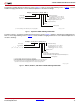
Stacked Silicon Interconnect (SSI) Technology
There are many challenges associated with creating high capacity FPGAs that Xilinx addresses with the SSI technology.
SSI technology enables multiple super logic regions (SLRs) to be combined on a passive interposer layer, using proven
manufacturing and assembly techniques from industry leaders, to create a single FPGA with more than ten thousand inter-
SLR connections, providing ultra-high bandwidth connectivity with low latency and low power consumption. There are two
types of SLRs used in Virtex-7 FPGAs: a logic intensive SLR used in the Virtex-7 T devices and a DSP/block
RAM/transceiver-rich SLR used in the Virtex-7 XT and HT devices. SSI technology enables the production of higher
capability FPGAs than traditional manufacturing methods, enabling the highest capacity and highest performance FPGAs
ever created to reach production more quickly and with less risk than would otherwise be possible. Thousands of super long
line (SLL) routing resources and ultra-high performance clock lines that cross between the SLRs ensure that designs span
seamlessly across these high-density programmable logic devices.
CLBs, Slices, and LUTs
Some key features of the CLB architecture include:
• Real 6-input look-up tables (LUTs)
• Memory capability within the LUT
• Register and shift register functionality
The LUTs in 7 series FPGAs can be configured as either one 6-input LUT (64-bit ROMs) with one output, or as two 5-input
LUTs (32-bit ROMs) with separate outputs but common addresses or logic inputs. Each LUT output can optionally be
registered in a flip-flop. Four such LUTs and their eight flip-flops as well as multiplexers and arithmetic carry logic form a
slice, and two slices form a configurable logic block (CLB). Four of the eight flip-flops per slice (one per LUT) can optionally
be configured as latches.
Between 25–50% of all slices can also use their LUTs as distributed 64-bit RAM or as 32-bit shift registers (SRL32) or as two
SRL16s. Modern synthesis tools take advantage of these highly efficient logic, arithmetic, and memory features.
Clock Management
Some of the key highlights of the clock management architecture include:
• High-speed buffers and routing for low-skew clock distribution
• Frequency synthesis and phase shifting
• Low-jitter clock generation and jitter filtering
Each 7 series FPGA has up to 24 clock management tiles (CMTs), each consisting of one mixed-mode clock manager
(MMCM) and one phase-locked loop (PLL).
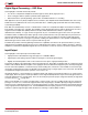
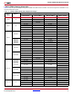
Table 11: Virtex-7 HT FPGA Device-Package Combinations and Maximum I/Os
Package
(1)
FLG1155 FLG1931 FLG1932
Size (mm) 35 x 35 45 x 45 45 x 45
Ball Pitch 1.0 1.0 1.0
Device GTH GTZ
I/O
GTH GTZ
I/O
GTH GTZ
I/O
HP
(2)
HP
(2)
HP
(2)
XC7VH580T 24 8 400 48 8 600
XC7VH870T 72 16 300
Notes:
1. All packages listed are Pb-free with exemption 15. Some packages are available in Pb option.
2. HP = High-performance I/O with support for I/O voltage from 1.2V to 1.8V.