
Datasheet

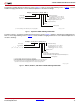

7 Series FPGAs Data Sheet: Overview
DS180 (v2.5) August 1, 2017 www.xilinx.com
Product Specification 8
Mixed-Mode Clock Manager and Phase-Locked Loop
The MMCM and PLL share many characteristics. Both can serve as a frequency synthesizer for a wide range of frequencies
and as a jitter filter for incoming clocks. At the center of both components is a voltage-controlled oscillator (VCO), which
speeds up and slows down depending on the input voltage it receives from the phase frequency detector (PFD).
There are three sets of programmable frequency dividers: D, M, and O. The pre-divider D (programmable by configuration
and afterwards via DRP) reduces the input frequency and feeds one input of the traditional PLL phase/frequency
comparator. The feedback divider M (programmable by configuration and afterwards via DRP) acts as a multiplier because
it divides the VCO output frequency before feeding the other input of the phase comparator. D and M must be chosen
appropriately to keep the VCO within its specified frequency range. The VCO has eight equally-spaced output phases
(0°, 45°, 90°, 135°, 180°, 225°, 270°, and 315°). Each can be selected to drive one of the output dividers (six for the PLL,
O0 to O5, and seven for the MMCM, O0 to O6), each programmable by configuration to divide by any integer from 1 to 128.
The MMCM and PLL have three input-jitter filter options: low bandwidth, high bandwidth, or optimized mode. Low-bandwidth
mode has the best jitter attenuation but not the smallest phase offset. High-bandwidth mode has the best phase offset, but
not the best jitter attenuation. Optimized mode allows the tools to find the best setting.
MMCM Additional Programmable Features
The MMCM can have a fractional counter in either the feedback path (acting as a multiplier) or in one output path. Fractional
counters allow non-integer increments of
1
/8 and can thus increase frequency synthesis capabilities by a factor of 8.
The MMCM can also provide fixed or dynamic phase shift in small increments that depend on the VCO frequency. At
1600 MHz, the phase-shift timing increment is 11.2 ps.
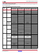
Clock Distribution
Each 7 series FPGA provides six different types of clock lines (BUFG, BUFR, BUFIO, BUFH, BUFMR, and the high-
performance clock) to address the different clocking requirements of high fanout, short propagation delay, and extremely low
skew.
Global Clock Lines
In each 7 series FPGA (except XC7S6 and XC7S15), 32 global clock lines have the highest fanout and can reach every flip-
flop clock, clock enable, and set/reset, as well as many logic inputs. There are 12 global clock lines within any clock region
driven by the horizontal clock buffers (BUFH). Each BUFH can be independently enabled/disabled, allowing for clocks to be
turned off within a region, thereby offering fine-grain control over which clock regions consume power. Global clock lines can
be driven by global clock buffers, which can also perform glitchless clock multiplexing and clock enable functions. Global
clocks are often driven from the CMT, which can completely eliminate the basic clock distribution delay.
Regional Clocks
Regional clocks can drive all clock destinations in their region. A region is defined as an area that is 50 I/O and 50 CLB high
and half the chip wide. 7 series FPGAs have between two and twenty-four regions. There are four regional clock tracks in
every region. Each regional clock buffer can be driven from any of four clock-capable input pins, and its frequency can
optionally be divided by any integer from 1 to 8.
I/O Clocks
I/O clocks are especially fast and serve only I/O logic and serializer/deserializer (SerDes) circuits, as described in the
I/O Logic section. The 7 series devices have a direct connection from the MMCM to the I/O for low-jitter, high-performance
interfaces.