
Datasheet


DS189 (v1.2) June 20, 2017 www.xilinx.com
Preliminary Product Specification 1
Introduction
Spartan®-7 FPGAs are available in -2, -1, and -1L speed grades, with -2 having the highest performance.
The Spartan-7 FPGAs predominantly operate at a 1.0V core voltage. The -1L devices are screened for lower
maximum static power and can operate at lower core voltages for lower dynamic power than the -1
devices. The -1L devices operate only at V
CCINT
=V
CCBRAM
= 0.95V and have the same speed
specifications as the -1 speed grade.
Spartan-7 FPGA DC and AC characteristics are specified in commercial and industrial temperature ranges.
Except the operating temperature range or unless otherwise noted, all the DC and AC electrical
parameters are the same for a particular speed grade (that is, the timing characteristics of a -1I industrial
speed grade device are the same as for a -1C commercial speed grade device). However, only selected
speed grades and/or devices are available in each temperature range. For example, the -1L speed grade is
only available in the industrial (I) temperature range.
All supply voltage and junction temperature specifications are representative of worst-case conditions.
The parameters included are common to popular designs and typical applications.
Available device and package combinations can be found in the 7 Series FPGAs Overview (DS180) [Ref 1].
This Spartan-7 FPGA data sheet, part of an overall set of documentation on the 7 series FPGAs, is available
on the Xilinx website at www.xilinx.com/documentation
.
DC Characteristics
Spartan-7 FPGAs Data Sheet:
DC and AC Switching Characteristics
DS189 (v1.2) June 20, 2017
Preliminary Product Specification
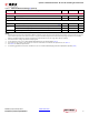
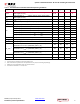
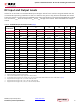
Table 1: Absolute Maximum Ratings
(1)
Symbol Description Min Max Units
FPGA Logic
V
CCINT
Internal supply voltage. –0.5 1.1 V
V
CCAUX
Auxiliary supply voltage. –0.5 2.0 V
V
CCBRAM
Supply voltage for the block RAM memories. –0.5 1.1 V
V
CCO
Output drivers supply voltage for HR I/O banks. –0.5 3.6 V
V
REF
Input reference voltage. –0.5 2.0 V
V
IN
(2)(3)(4)
I/O input voltage. –0.4 V
CCO
+0.55 V
I/O input voltage (when V
CCO
=3.3V) for V
REF
and differential I/O
standards except TMDS_33.
(5)
–0.4 2.625 V
V
CCBATT
Key memory battery backup supply. –0.5 2.0 V