
Datasheet


Spartan-7 FPGAs Data Sheet: DC and AC Switching Characteristics
DS189 (v1.2) June 20, 2017 www.xilinx.com
Preliminary Product Specification 3
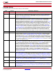
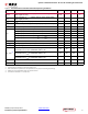
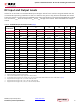
Table 2: Recommended Operating Conditions
(1)(2)
Symbol Description Min Typ Max Units
FPGA Logic
V
CCINT
(3)
For -2 and -1 (1.0V) devices: internal supply voltage. 0.95 1.00 1.05 V
For -1L (0.95V) devices: internal supply voltage. 0.92 0.95 0.98 V
V
CCAUX
Auxiliary supply voltage. 1.71 1.80 1.89 V
V
CCBRAM
(3)
For -2 and -1 (1.0V) devices: block RAM supply voltage. 0.95 1.00 1.05 V
For -1L (0.95V) devices: block RAM supply voltage. 0.92 0.95 0.98 V
V
CCO
(4)(5)
Supply voltage for HR I/O banks. 1.14 – 3.465 V
V
IN
(6)
I/O input voltage. –0.20 – V
CCO
+0.20 V
I/O input voltage (when V
CCO
= 3.3V) for V
REF
and
differential I/O standards except TMDS_33.
(7)
–0.20 – 2.625 V
I
IN
(8)
Maximum current through any pin in a powered or unpowered
bank when forward biasing the clamp diode.
–– 10 mA
V
CCBATT
(9)
Battery voltage. 1.0 – 1.89 V
XADC
V
CCADC
XADC supply relative to GNDADC. 1.71 1.80 1.89 V
V
REFP
Externally supplied reference voltage. 1.20 1.25 1.30 V
Temperature
T
j
Junction temperature operating range for commercial (C)
temperature devices.
0– 85 °C
Junction temperature operating range for industrial (I)
temperature devices.
–40 – 100 °C
Notes:
1. All voltages are relative to ground.
2. For the design of the power distribution system consult the 7 Series FPGAs PCB Design Guide (UG483) [Ref 4].
3. If V
CCINT
and V
CCBRAM
are operating at the same voltage, V
CCINT
and V
CCBRAM
should be connected to the same supply.
4. Configuration data is retained even if V
CCO
drops to 0V.
5. Includes V
CCO
of 1.2V, 1.35V, 1.5V, 1.8V, 2.5V, and 3.3V at ±5%.
6. The lower absolute voltage specification always applies.
7. See Table 9 for TMDS_33 specifications.
8. A total of 200 mA per bank should not be exceeded.
9. V
CCBATT
is required only when using bitstream encryption. If battery is not used, connect V
CCBATT
to either ground or V
CCAUX
.