
Datasheet


Spartan-7 FPGAs Data Sheet: DC and AC Switching Characteristics
DS189 (v1.2) June 20, 2017 www.xilinx.com
Preliminary Product Specification 6
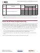
Power-On/Off Power Supply Sequencing
The recommended power-on sequence is V
CCINT
, V
CCBRAM
, V
CCAUX
, and V
CCO
to achieve minimum current
draw and ensure that the I/Os are 3-stated at power-on. The recommended power-off sequence is the
reverse of the power-on sequence. If V
CCINT
and V
CCBRAM
have the same recommended voltage levels then
both can be powered by the same supply and ramped simultaneously. If V
CCAUX
and V
CCO
have the same
recommended voltage levels then both can be powered by the same supply and ramped simultaneously.
For V
CCO
voltages of 3.3V in HR I/O banks and configuration bank 0 the following conditions apply.
• The voltage difference between V
CCO
and V
CCAUX
must not exceed 2.625V for longer than
T
VCCO2VCCAUX
for each power-on/off cycle to maintain device reliability levels.
• The T
VCCO2VCCAUX
time can be allocated in any percentage between the power-on and power-off
ramps.
There is no recommended sequence for supplies not discussed in this section.
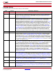
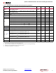
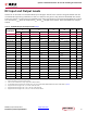
I
CCBRAMQ
Quiescent V
CCBRAM
supply current.
XC7S6 mA
XC7S15 mA
XC7S25 2 2 1 mA
XC7S50 2 2 1 mA
XC7S75 mA
XC7S100 mA
Notes:
1. Typical values are specified at nominal voltage, 85°C junction temperature (T
j
) with single-ended SelectIO™ resources.
2. Typical values are for blank configured devices with no output current loads, no active input pull-up resistors, all I/O pins are 3-state and
floating.
3. Use the Xilinx Power Estimator spreadsheet tool [Ref 5] to estimate static power consumption for conditions other than those specified.
Table 5: Typical Quiescent Supply Current
(1)(2)(3)
(Cont’d)
Symbol Description Device
Speed Grade
Units1.0V 0.95V
-2C/-2I -1C/-1I -1LI