
Datasheet


Spartan-7 FPGAs Data Sheet: DC and AC Switching Characteristics
DS189 (v1.2) June 20, 2017 www.xilinx.com
Preliminary Product Specification 7
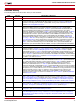
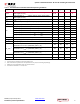
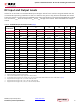
Table 6 shows the minimum current, in addition to I
CCQ
maximum, that is required by Spartan-7 devices for
proper power-on and configuration. If the current minimums shown in Table 6 are met, the device powers
on after all four supplies have passed through their power-on reset threshold voltages. The FPGA must not
be configured until after V
CCINT
is applied. Once initialized and configured, use the Xilinx Power Estimator
spreadsheet tool [Ref 5] to estimate current drain on these supplies.
Table 6: Power-On Current for Spartan-7 Devices
Device I
CCINTMIN
I
CCAUXMIN
I
CCOMIN
I
CCBRAMMIN
Units
XC7S6 I
CCINTQ
+ 120 I
CCAUXQ
+ 40 I
CCOQ
+ 40 mA per bank I
CCBRAMQ
+ 60 mA
XC7S15 I
CCINTQ
+ 120 I
CCAUXQ
+ 40 I
CCOQ
+ 40 mA per bank I
CCBRAMQ
+ 60 mA
XC7S25 I
CCINTQ
+ 120 I
CCAUXQ
+ 40 I
CCOQ
+ 40 mA per bank I
CCBRAMQ
+ 60 mA
XC7S50 I
CCINTQ
+ 120 I
CCAUXQ
+ 40 I
CCOQ
+ 40 mA per bank I
CCBRAMQ
+ 60 mA
XC7S75 I
CCINTQ
+ 170 I
CCAUXQ
+ 40 I
CCOQ
+ 40 mA per bank I
CCBRAMQ
+ 60 mA
XC7S100 I
CCINTQ
+ 170 I
CCAUXQ
+ 40 I
CCOQ
+ 40 mA per bank I
CCBRAMQ
+ 60 mA
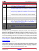
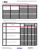
Table 7: Power Supply Ramp Time
Symbol Description Conditions Min Max Units
T
VCCINT
Ramp time from GND to 90% of V
CCINT
.0.250ms
T
VCCO
Ramp time from GND to 90% of V
CCO
.0.250ms
T
VCCAUX
Ramp time from GND to 90% of V
CCAUX
.0.250ms
T
VCCBRAM
Ramp time from GND to 90% of V
CCBRAM
.0.250ms
T
VCCO2VCCAUX
Allowed time per power cycle for V
CCO
–V
CCAUX
> 2.625V.
T
J
=125°C
(1)
– 300 ms
T
J
=100°C
(1)
– 500 ms
T
J
=85°C
(1)
– 800 ms
Notes:
1. Based on 240,000 power cycles with a nominal V
CCO
of 3.3V or 36,500 power cycles with a worst case V
CCO
of 3.465V.