
Datasheet
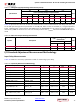

Spartan-7 FPGAs Data Sheet: DC and AC Switching Characteristics
DS189 (v1.2) June 20, 2017 www.xilinx.com
Preliminary Product Specification 14
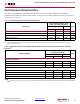
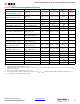
IOB Pad Input/Output/3-State
Table 17 summarizes the values of standard-specific data input delay adjustments, output delays
terminating at pads (based on standard) and 3-state delays.
• T
IOPI
is described as the delay from IOB pad through the input buffer to the I-pin of an IOB pad. The
delay varies depending on the capability of the SelectIO input buffer.
• T
IOOP
is described as the delay from the O pin to the IOB pad through the output buffer of an IOB
pad. The delay varies depending on the capability of the SelectIO output buffer.
• T
IOTP
is described as the delay from the T pin to the IOB pad through the output buffer of an IOB pad,
when 3-state is disabled. The delay varies depending on the SelectIO capability of the output buffer.
In HR I/O banks, the IN_TERM termination turn-on time is always faster than T
IOTP
when the
INTERMDISABLE pin is used.
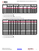
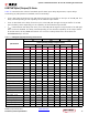
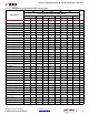
Table 17: IOB High Range (HR) Switching Characteristics
I/O Standard
T
IOPI
T
IOOP
T
IOTP
Units
V
CCINT
Operating Voltage and Speed Grade
1.0V 0.95V 1.0V 0.95V 1.0V 0.95V
-2 -1 -1L -2 -1 -1L -2 -1 -1L
LVTTL_S4 1.34 1.41 1.41 3.93 4.18 4.18 3.96 4.20 4.20 ns
LVTTL_S8 1.34 1.41 1.41 3.66 3.92 3.92 3.69 3.93 3.93 ns
LVTTL_S12 1.341.411.413.653.903.903.683.913.91ns
LVTTL_S16 1.341.411.413.193.453.453.223.463.46ns
LVTTL_S24 1.341.411.413.413.673.673.443.683.68ns
LVTTL_F4 1.34 1.41 1.41 3.38 3.64 3.64 3.41 3.65 3.65 ns
LVTTL_F8 1.34 1.41 1.41 2.87 3.12 3.12 2.90 3.13 3.13 ns
LVTTL_F12 1.341.411.412.853.103.102.883.123.12ns
LVTTL_F16 1.341.411.412.682.932.932.712.952.95ns
LVTTL_F24 1.341.411.412.652.902.902.682.912.91ns
LVDS_25 0.810.880.881.411.671.671.441.681.68ns
MINI_LVDS_25 0.81 0.88 0.88 1.40 1.65 1.65 1.43 1.66 1.66 ns
BLVDS_25 0.81 0.88 0.88 1.96 2.21 2.21 1.99 2.23 2.23 ns
RSDS_25 (point to point) 0.81 0.88 0.88 1.40 1.65 1.65 1.43 1.66 1.66 ns
PPDS_25 0.810.880.881.411.671.671.441.681.68ns
TMDS_33 0.810.880.881.541.791.791.571.801.80ns
PCI33_3 1.321.391.393.223.483.483.253.493.49ns
HSUL_12_S 0.750.820.821.932.182.181.962.202.20ns
HSUL_12_F 0.750.820.821.411.671.671.441.681.68ns
DIFF_HSUL_12_S 0.76 0.83 0.83 1.93 2.18 2.18 1.96 2.20 2.20 ns
DIFF_HSUL_12_F 0.76 0.83 0.83 1.41 1.67 1.67 1.44 1.68 1.68 ns
MOBILE_DDR_S 0.84 0.91 0.91 1.80 2.06 2.06 1.83 2.07 2.07 ns
MOBILE_DDR_F 0.84 0.91 0.91 1.51 1.76 1.76 1.54 1.77 1.77 ns
DIFF_MOBILE_DDR_S 0.78 0.85 0.85 1.82 2.07 2.07 1.85 2.09 2.09 ns