
Datasheet

Spartan-7 FPGAs Data Sheet: DC and AC Switching Characteristics
DS189 (v1.2) June 20, 2017 www.xilinx.com
Preliminary Product Specification 17
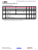
Table 18 specifies the values of T
IOTPHZ
and T
IOIBUFDISABLE
. T
IOTPHZ
is described as the delay from the T pin
to the IOB pad through the output buffer of an IOB pad, when 3-state is enabled (i.e., a high impedance
state). T
IOIBUFDISABLE
is described as the IOB delay from IBUFDISABLE to O output. In HR I/O banks, the
internal IN_TERM termination turn-off time is always faster than T
IOTPHZ
when the INTERMDISABLE pin is
used.
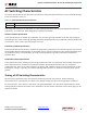
I/O Standard Adjustment Measurement Methodology
Input Delay Measurements
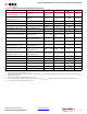
Table 19 shows the test setup parameters used for measuring input delay.
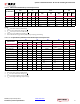
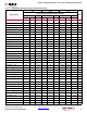
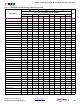
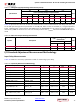
DIFF_SSTL18_I_F 0.79 0.86 0.86 1.35 1.60 1.60 1.38 1.62 1.62 ns
DIFF_SSTL18_II_F 0.790.860.861.331.591.591.361.601.60ns
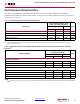
Table 18: IOB 3-state Output Switching Characteristics
Symbol Description
V
CCINT
Operating Voltage and
Speed Grade
Units
1.0V 0.95V
-2 -1 -1L
T
IOTPHZ
T input to pad high-impedance. 2.19 2.37 2.37 ns
T
IOIBUFDISABLE
IBUF turn-on time from IBUFDISABLE to O output. 2.30 2.60 2.60 ns
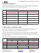
Table 19: Input Delay Measurement Methodology
Description I/O Standard Attribute V
L
(1)
V
H
(1)
V
MEAS
(3)(5)
V
REF
(2)(4)
LVCMOS, 1.2V LVCMOS12 0.1 1.1 0.6 –
LVCMOS, 1.5V LVCMOS15 0.1 1.4 0.75 –
LVCMOS, 1.8V LVCMOS18 0.1 1.7 0.9 –
LVCMOS, 2.5V LVCMOS25 0.1 2.4 1.25 –
LVCMOS, 3.3V LVCMOS33 0.1 3.2 1.65 –
LVTTL, 3.3V LVTTL 0.1 3.2 1.65 –
MOBILE_DDR, 1.8V MOBILE_DDR 0.1 1.7 0.9 –
PCI33, 3.3V PCI33_3 0.1 3.2 1.65 –
HSTL (high-speed transceiver
logic), Class I, 1.2V
HSTL_I_12 V
REF
–0.5 V
REF
+0.5 V
REF
0.60
HSTL, Class I & II, 1.5V HSTL_I, HSTL_II V
REF
–0.65 V
REF
+0.65 V
REF
0.75
HSTL, Class I & II, 1.8V
HSTL_I_18,
HSTL_II_18
V
REF
–0.8 V
REF
+0.8 V
REF
0.90
Table 17: IOB High Range (HR) Switching Characteristics (Cont’d)
I/O Standard
T
IOPI
T
IOOP
T
IOTP
Units
V
CCINT
Operating Voltage and Speed Grade
1.0V 0.95V 1.0V 0.95V 1.0V 0.95V
-2 -1 -1L -2 -1 -1L -2 -1 -1L