
Datasheet


Spartan-7 FPGAs Data Sheet: DC and AC Switching Characteristics
DS189 (v1.2) June 20, 2017 www.xilinx.com
Preliminary Product Specification 35
Clock Buffers and Networks
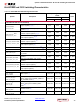
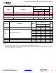
Table 32: Global Clock Switching Characteristics (Including BUFGCTRL)
Symbol Description
V
CCINT
Operating Voltage and
Speed Grade
Units
1.0V 0.95V
-2 -1 -1L
T
BCCCK_CE
/T
BCCKC_CE
(1)
CE pins setup/hold. 0.13/0.40 0.16/0.41 0.16/0.41 ns
T
BCCCK_S
/ T
BCCKC_S
(1)
S pins setup/hold. 0.13/0.40 0.16/0.41 0.16/0.41 ns
T
BCCKO_O
(2)
BUFGCTRL delay from I0/I1 to O. 0.09 0.10 0.10 ns
Maximum Frequency
F
MAX_BUFG
Global clock tree (BUFG). 628.00 464.00 464.00 MHz
Notes:
1. T
BCCCK_CE
and T
BCCKC_CE
must be satisfied to assure glitch-free operation of the global clock when switching between clocks. These
parameters do not apply to the BUFGMUX primitive that assures glitch-free operation. The other global clock setup and hold times are
optional; only needing to be satisfied if device operation requires simulation matches on a cycle-for-cycle basis when switching between
clocks.
2. T
BGCKO_O
(BUFG delay from I0 to O) values are the same as T
BCCKO_O
values.
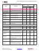
Table 33: Input/Output Clock Switching Characteristics (BUFIO)
Symbol Description
V
CCINT
Operating Voltage and
Speed Grade
Units
1.0V 0.95V
-2 -1 -1L
T
BIOCKO_O
Clock to out delay from I to O. 1.26 1.54 1.54 ns
Maximum Frequency
F
MAX_BUFIO
I/O clock tree (BUFIO). 680.00 600.00 600.00 MHz
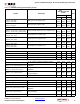
Table 34: Regional Clock Buffer Switching Characteristics (BUFR)
Symbol Description
V
CCINT
Operating Voltage and
Speed Grade
Units
1.0V 0.95V
-2 -1 -1L
T
BRCKO_O
Clock to out delay from I to O. 0.76 0.99 0.99 ns
T
BRCKO_O_BYP
Clock to out delay from I to O with Divide Bypass
attribute set.
0.39 0.52 0.52 ns
T
BRDO_O
Propagation delay from CLR to O. 0.85 1.09 1.09 ns
Maximum Frequency
F
MAX_BUFR
(1)
Regional clock tree (BUFR). 375.00 315.00 315.00 MHz
Notes:
1. The maximum input frequency to the BUFR is the BUFIO F
MAX
frequency.