
Datasheet


Spartan-7 FPGAs Data Sheet: DC and AC Switching Characteristics
DS189 (v1.2) June 20, 2017 www.xilinx.com
Preliminary Product Specification 36
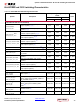
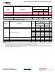
Table 35: Horizontal Clock Buffer Switching Characteristics (BUFH)
Symbol Description
V
CCINT
Operating Voltage and Speed
Grade
Units
1.0V 0.95V
-2 -1 -1L
T
BHCKO_O
BUFH delay from I to O. 0.11 0.13 0.13 ns
T
BHCCK_CE
/ T
BHCKC_CE
CE pin setup and hold. 0.22/0.15 0.28/0.21 0.28/0.21 ns
Maximum Frequency
F
MAX_BUFH
Horizontal clock buffer (BUFH). 628.00 464.00 464.00 MHz
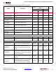
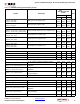
Table 36: Duty Cycle Distortion and Clock-Tree Skew
Symbol Description Device
V
CCINT
Operating Voltage and
Speed Grade
Units
1.0V 0.95V
-2 -1 -1L
T
DCD_CLK
Global clock tree duty-cycle distortion.
(1)
All 0.20 0.20 0.20 ns
T
CKSKEW
Global clock tree skew.
(2)
XC7S6 0.05 0.06 0.06 ns
XC7S15 0.05 0.06 0.06 ns
XC7S25 0.26 0.26 0.26 ns
XC7S50 0.26 0.26 0.26 ns
XC7S75 0.33 0.36 0.36 ns
XC7S100 0.33 0.36 0.36 ns
T
DCD_BUFIO
I/O clock tree duty cycle distortion. All 0.14 0.14 0.14 ns
T
BUFIOSKEW
I/O clock tree skew across one clock region. All 0.03 0.03 0.03 ns
T
DCD_BUFR
Regional clock tree duty cycle distortion. All 0.18 0.18 0.18 ns
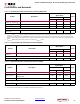
Notes:
1. These parameters represent the worst-case duty cycle distortion observable at the I/O flip flops. For all I/O standards, IBIS can be used to
calculate any additional duty cycle distortion that might be caused by asymmetrical rise/fall times.
2. The T
CKSKEW
value represents the worst-case clock-tree skew observable between sequential I/O elements. Significantly less clock-tree skew
exists for I/O registers that are close to each other and fed by the same or adjacent clock-tree branches. Use the Xilinx timing analysis tools
to evaluate clock skew specific to your application.