
Datasheet


7 Series FPGAs Data Sheet: Overview
DS180 (v2.5) August 1, 2017 www.xilinx.com
Product Specification 2
Spartan-7 FPGA Feature Summary
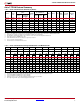
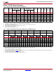
Table 2: Spartan-7 FPGA Feature Summary by Device
Device
Logic
Cells
CLB
DSP
Slices
(2)
Block RAM Blocks
(3)
CMTs
(4)
PCIe GT
XADC
Blocks
Total I/O
Banks
(5)
Max User
I/O
Slices
(1)
Max
Distributed
RAM (Kb)
18 Kb 36 Kb
Max
(Kb)
XC7S6 6,000 938 70 10 10 5 180 2 0 0 0 2 100
XC7S15 12,800 2,000 150 20 20 10 360 2 0 0 0 2 100
XC7S25 23,360 3,650 313 80 90 45 1,620 3 0 0 1 3 150
XC7S50 52,160 8,150 600 120 150 75 2,700 5 0 0 1 5 250
XC7S75 76,800 12,000 832 140 180 90 3,240 8 0 0 1 8 400
XC7S100 102,400 16,000 1,100 160 240 120 4,320 8 0 0 1 8 400
Notes:
1. Each 7 series FPGA slice contains four LUTs and eight flip-flops; only some slices can use their LUTs as distributed RAM or SRLs.
2. Each DSP slice contains a pre-adder, a 25 x 18 multiplier, an adder, and an accumulator.
3. Block RAMs are fundamentally 36 Kb in size; each block can also be used as two independent 18 Kb blocks.
4. Each CMT contains one MMCM and one PLL.
5. Does not include configuration Bank 0.
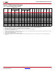
Table 3: Spartan-7 FPGA Device-Package Combinations and Maximum I/Os
Package CPGA196 CSGA225 CSGA324 FTGB196 FGGA484 FGGA676
Size (mm) 8 x 8 13 x 13 15 x 15 15 x 15 23 x 23 27 x 27
Ball Pitch (mm)0.50.80.81.01.01.0
Device HR I/O
(1)
HR I/O
(1)
HR I/O
(1)
HR I/O
(1)
HR I/O
(1)
HR I/O
(1)
XC7S6 100 100 100
XC7S15 100 100 100
XC7S25 150 150 100
XC7S50 210 100 250
XC7S75 338 400
XC7S100
338 400
Notes:
1. HR = High-range I/O with support for I/O voltage from 1.2V to 3.3V.