
Datasheet

Spartan-7 FPGAs Data Sheet: DC and AC Switching Characteristics
DS189 (v1.2) June 20, 2017 www.xilinx.com
Preliminary Product Specification 40
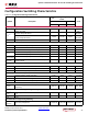
Device Pin-to-Pin Output Parameter Guidelines
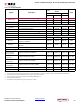
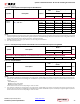
Table 39: Clock-Capable Clock Input to Output Delay Without MMCM/PLL (Near Clock Region)
(1)
Symbol Description Device
V
CCINT
Operating Voltage and
Speed Grade
Units
1.0V 0.95V
-2 -1 -1L
SSTL15 Clock-Capable Clock Input to Output Delay using Output Flip-Flop, Fast Slew Rate, without MMCM/PLL.
T
ICKOF
Clock-capable clock input and OUTFF at
pins/banks closest to the BUFGs without
MMCM/PLL (near clock region).
(2)
XC7S6 5.556.506.50ns
XC7S15 5.55 6.50 6.50 ns
XC7S25 5.55 6.44 6.44 ns
XC7S50 5.71 6.62 6.62 ns
XC7S75 5.73 6.71 6.71 ns
XC7S1005.736.716.71ns
Notes:
1. This table lists representative values where one global clock input drives one vertical clock line in each accessible column, and where all
accessible IOB and CLB flip-flops are clocked by the global clock net.
2. Refer to the Die Level Bank Numbering Overview section of the 7 Series FPGA Packaging and Pinout Specification (UG475) [Ref 3].
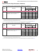
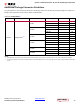
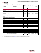
Table 40: Clock-Capable Clock Input to Output Delay Without MMCM/PLL (Far Clock Region)
(1)
Symbol Description Device
V
CCINT
Operating Voltage and
Speed Grade
Units
1.0V 0.95V
-2 -1 -1L
SSTL15 Clock-Capable Clock Input to Output Delay using Output Flip-Flop, Fast Slew Rate, without MMCM/PLL.
T
ICKOFFAR
Clock-capable clock input and OUTFF at
pins/banks farthest from the BUFGs without
MMCM/PLL (far clock region).
(2)
XC7S6 5.55 6.50 6.50 ns
XC7S15 5.55 6.50 6.50 ns
XC7S25 5.55 6.44 6.44 ns
XC7S50 5.71 6.62 6.62 ns
XC7S75 6.01 7.02 7.02 ns
XC7S100 6.01 7.02 7.02 ns
Notes:
1. This table lists representative values where one global clock input drives one vertical clock line in each accessible column, and where all
accessible IOB and CLB flip-flops are clocked by the global clock net.
2. Refer to the Die Level Bank Numbering Overview section of the 7 Series FPGA Packaging and Pinout Specification (UG475) [Ref 3].