
Datasheet

Spartan-7 FPGAs Data Sheet: DC and AC Switching Characteristics
DS189 (v1.2) June 20, 2017 www.xilinx.com
Preliminary Product Specification 41
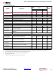
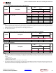
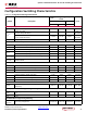
Table 41: Clock-Capable Clock Input to Output Delay With MMCM
(1)
Symbol Description Device
V
CCINT
Operating Voltage and
Speed Grade
Units
1.0V 0.95V
-2 -1 -1L
SSTL15 Clock-Capable Clock Input to Output Delay using Output Flip-Flop, Fast Slew Rate, with MMCM.
T
ICKOFMMCMCC
Clock-capable clock input and OUTFF with
MMCM.
(2)
XC7S6 1.03 1.03 1.03 ns
XC7S15 1.03 1.03 1.03 ns
XC7S25 1.00 1.00 1.00 ns
XC7S50 1.00 1.00 1.00 ns
XC7S75 1.00 1.00 1.00 ns
XC7S100 1.00 1.00 1.00 ns
Notes:
1. This table lists representative values where one global clock input drives one vertical clock line in each accessible column, and where all
accessible IOB and CLB flip-flops are clocked by the global clock net.
2. MMCM output jitter is already included in the timing calculation.
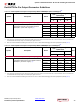
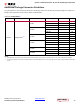
Table 42: Clock-Capable Clock Input to Output Delay With PLL
(1)
Symbol Description Device
V
CCINT
Operating Voltage and
Speed Grade
Units
1.0V 0.95V
-2 -1 -1L
SSTL15 Clock-Capable Clock Input to Output Delay using Output Flip-Flop, Fast Slew Rate, with PLL.
T
ICKOFPLLCC
Clock-capable clock input and OUTFF with
PLL.
(2)
XC7S6 0.85 0.85 0.85 ns
XC7S15 0.85 0.85 0.85 ns
XC7S25 0.83 0.83 0.83 ns
XC7S50 0.83 0.83 0.83 ns
XC7S75 0.83 0.83 0.83 ns
XC7S100 0.83 0.83 0.83 ns
Notes:
1. This table lists representative values where one global clock input drives one vertical clock line in each accessible column, and where all
accessible IOB and CLB flip-flops are clocked by the global clock net.
2. PLL output jitter is already included in the timing calculation.
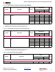
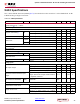
Table 43: Pin-to-Pin, Clock-to-Out using BUFIO
Symbol Description
V
CCINT
Operating Voltage and Speed
Grade
Units
1.0V 0.95V
-2 -1 -1L
SSTL15 Clock-Capable Clock Input to Output Delay using Output Flip-Flop, Fast Slew Rate, with BUFIO.
T
ICKOFCS
Clock to out of I/O clock. 5.61 6.64 6.64 ns