
Datasheet

Spartan-7 FPGAs Data Sheet: DC and AC Switching Characteristics
DS189 (v1.2) June 20, 2017 www.xilinx.com
Preliminary Product Specification 43
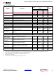
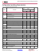
Table 46: Clock-Capable Clock Input Setup and Hold With PLL
Symbol Description Device
V
CCINT
Operating Voltage and Speed
Grade
Units
1.0V 0.95V
-2 -1 -1L
Input Setup and Hold Time Relative to Clock-Capable Clock Input Signal for SSTL15 Standard.
(1)(2)
T
PSPLLCC
/
T
PHPLLCC
No delay clock-capable clock input and
IFF
(3)
with PLL.
XC7S6 3.07/–0.17 3.69/–0.17 3.69/–0.17 ns
XC7S15 3.07/–0.17 3.69/–0.17 3.69/–0.17 ns
XC7S25 3.04/–0.19 3.63/–0.19 3.63/–0.19 ns
XC7S50 3.15/–0.19 3.77/–0.19 3.77/–0.19 ns
XC7S75 3.15/–0.19 3.78/–0.19 3.78/–0.19 ns
XC7S100 3.15/–0.19 3.78/–0.19 3.78/–0.19 ns
Notes:
1. Setup and hold times are measured over worst case conditions (process, voltage, temperature). Setup time is measured relative to the global
clock input signal using the slowest process, highest temperature, and lowest voltage. Hold time is measured relative to the global clock input
signal using the fastest process, lowest temperature, and highest voltage.
2. Use IBIS to determine any duty-cycle distortion incurred using various standards.
3. IFF = Input flip-flop or latch.
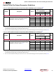
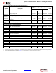
Table 47: Data Input Setup and Hold Times Relative to a Forwarded Clock Input Pin Using BUFIO
Symbol Description
V
CCINT
Operating Voltage and Speed
Grade
Units
1.0V 0.95V
-2 -1 -1L
Input Setup and Hold Time Relative to a Forwarded Clock Input Pin Using BUFIO for SSTL15 Standard.
T
PSCS
/T
PHCS
Setup and hold of I/O clock. –0.38/1.46 –0.38/1.73 –0.38/1.76 ns
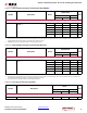
Table 48: Sample Window
Symbol Description
V
CCINT
Operating Voltage and Speed
Grade
Units
1.0V 0.95V
-2 -1 -1L
T
SAMP
Sampling error at receiver pins.
(1)
0.64 0.70 0.70 ns
T
SAMP_BUFIO
Sampling error at receiver pins using BUFIO.
(2)
0.40 0.46 0.46 ns
Notes:
1. This parameter indicates the total sampling error of the Spartan-7 FPGAs DDR input registers, measured across voltage, temperature, and
process. The characterization methodology uses the MMCM to capture the DDR input registers’ edges of operation. These measurements
include:
- CLK0 MMCM jitter
- MMCM accuracy (phase offset)
- MMCM phase shift resolution
These measurements do not include package or clock tree skew.
2. This parameter indicates the total sampling error of the Spartan-7 FPGAs DDR input registers, measured across voltage, temperature, and
process. The characterization methodology uses the BUFIO clock network and IDELAY to capture the DDR input registers’ edges of operation.
These measurements do not include package or clock tree skew.